estrutura atômica e eletrônica do óxido fosforeno: um novo...
TRANSCRIPT
CNPEM é uma Organização Social qualificada pelo Ministério da Ciência, Tecnologia, Inovações e Comunicações (MCTIC) Campus: Rua Giuseppe Máximo Scolfaro, 10.000 - Polo II de Alta Tecnologia - Caixa Postal 6192 - 13083-970 - Campinas/SP
Fone: +55.19.3512.1010 | Fax: +55.19.3512.1004 | www.cnpem.br
ProjetoparaBolsadeIniciaçãoCientíficaPIBIC/CNPEM
Estruturaatômicaeeletrônicadoóxidofosforeno:umnovomaterial2Dparananotransistores
Orientador:WendellSimõeseSilvaCo-orientadorTúlioC.R.RochaUnidadeLaboratórioNacionaldeLuzSíncrotronIntrodução
Ofosforenoéumnovoummaterialbidimensionalultrafino,similaraografeno,
mas formado por átomos de fósforo ao invés de carbono (figura 1-esquerda). Nos
últimosanos,ofosforenotemganhadomuitaatençãodacomunidadecientíficapois[1],
ao contrário do grafeno que é um excelente condutor de eletricidade, apresenta
propriedadesde transporte elétricodeumsemicondutor comoo silício, que é abase
atualde todaa indústriademicroeletrônica. Desta formaháumagrandeexpectativa
queo fosforenopossasubstituirosilíciode formadiretanaproduçãodedispositivos
eletrônicos em escala manométrica. De fato, alguns dispositivos experimentais
baseadosemfosforenojáforamconstruídos[2]parademonstrarseupotencial(figura
1-direita). Além disso, o fosforeno apresenta absorção óptica na região do
infravermelho próximo e visível, o que potencializa aplicações em dispositivos opto-
eletrônicosparacomunicaçõesópticas.
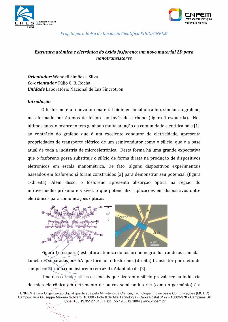
Figura1:(esquera)estruturaatômicadofósforononegroilustrandoascamadas
lamelaresseparadaspor5Aqueformamofosforeno.(direita)transisitorporefeitode
campoconstruídocomfósforeno(emazul).Adaptadode[2].
Umadascaracterísticasessenciaisque fizeramosilícioprevalecerna indústria
demicroeletrônica em detrimento de outros semicondutores (como o germânio) é a
dielectrics for higher doping. Meanwhile, a subthreshold swing of!5 V per decade is observed, which is much larger than the sub-threshold swing in commercial silicon-based devices (!70 mVper decade). We note that the subthreshold swing in our devicesvaries from sample to sample (from !3.7 V per decade to!13.3 V per decade) and is of the same order of magnitude asreported in multilayer MoS2 devices with a similar backgateconfiguration24,25. The rather big subthreshold swing is mainlyattributed to the large thickness of the SiO2 backgate dielectricthat we use, and multiple factors such as insulator layer thickness26,the Schottky barrier at the subthreshold region25 and sample–substrate interface state may also have an influence.
The switching off at the negative side of the Vg sweep isaccompanied by a slight turn-on at positive gate voltages, asshown in Fig. 2b. To further explore this ambipolar behaviour, wefabricated few-layer phosphorene devices with multiple electricalcontacts (Fig. 2c, inset) and performed Hall measurements usingtwo opposing contacts (V2 and V4, for example) perpendicular tothe drain–source current path to measure the transverse resistanceRxy. The Hall coefficient RH, defined as the slope of Rxy as a function
of external magnetic field B, reflects both the sign and density of thecharge carriers in the sample. As shown in Fig. 2c, a carrier signinversion is clearly observed in the on states, with positive andnegative gate voltages corresponding to hole and electron conduc-tion, respectively. This unambiguously shows that the ambipolarswitching of the devices is caused by Fermi level shifting from thevalence band into the conduction band.
The nature of the electrical conduction was probed further byperforming I–V measurements in a two-terminal configuration(Fig. 2a). As shown in Fig. 2d, the source–drain current Ids varieslinearly with Vds in the on state of the hole side, indicating anohmic contact in this region. Meanwhile, Ids versus Vds is stronglynonlinear on the electron side (Fig. 2d, inset), as is typical for semi-conducting channels with Schottky barriers at the contacts. Theobserved I–V characteristics can be readily explained by workfunc-tion mismatch between the metal contacts and few-layer phosphor-ene; the high workfunction of the metal electrodes causes holeaccumulation at the metal–semiconductor interface, which formsa low-resistance ohmic contact for the p-doped sample, while forthe n-doped sample a depletion region is formed at the interface,leading to Schottky barriers and thus nonlinear conduction. Thismodel also explains the observed disparity between conduction atthe electron and hole sides in all our samples (Fig. 2b) and iswidely accepted to describe the contact behaviour in MoS2 devices27.
For potential applications in digital and radiofrequency devices,saturation of the drain current is crucial in order to reach maximumpossible operation speeds23. By carefully choosing the ratio betweenchannel length and SiO2 layer thickness, a well-defined current sat-uration can be achieved in the high drain–source bias region(Fig. 3a). Meanwhile, the electrical contacts remain ohmic in thelinear region at low drain–source biases. The results shown inFig. 3a were obtained in the on state of the hole side of the conduc-tion in a 5 nm sample with a 4.5-mm-long channel on the 90 nmSiO2 gate dielectric. Such a well-developed saturation behaviour,which is absent in graphene-based FET devices23, is crucial forachieving high power gains. Coupled with the fact that ourchannel thickness is on the order of nanometres and thus robustagainst short-channel effects when the channel length is shrunkto the nanometre scale, our results suggest the high potential ofblack phosphorus in high-speed field-effect device applications.We note that the on state conductance of our device is relativelylow and the threshold source–drain bias is relatively high comparedto typical silicon-based devices. Both factors are attributed to thelong channel length in our current device. Better device perform-ance, that is, larger saturation current and lower threshold bias, isexpected if the channel length and the gate oxide thickness arereduced. Further investigations are needed to test the limit of thedevice performances of black phosphorus FETs.
Charge transport mechanism in black phosphorus thin flakeWe now turn to the characterization of field-effect mobility in few-layer phosphorene devices. Conductance G was measured as afunction of Vg and we extracted the field-effect mobility mFE inthe linear region of the transfer characteristics28:
mFE = LW
1Cg
dGd(Vg − Vth)
(1)
where L and W are the length and width of the channel, respectively,Cg is the capacitance per unit area, and Vth is the thresholdgate voltage. A hole mobility as high as 984 cm2 V21 s21 is obtainedon a 10 nm sample, as shown in Fig. 3b, and is found to be stronglythickness-dependent. Transfer characteristics of two other typicalsamples of different thicknesses (8 nm and 5 nm, with the 5 nmsample the same as measured in Fig. 3a) are also shown inFig. 3b. The conductance was measured in a four-terminal
a
b
5 Å
k (Å−1)
E −
E f (eV
)
0.6 0.4 0.2 0 0.2 0.4 0.6 0.8
0
−2
−4
−6
2
4
L ZU T’
L
T’U
Z
Figure 1 | Crystal and electronic structure of bulk black phosphorus.a, Atomic structure of black phosphorus. b, Band structure of bulk blackphosphorus mapped out by ARPES measurements. A bandgap is clearlyobserved. Superimposed on top are calculated bands of the bulk crystal.Blue solid and red dashed lines denote empty and filled bands, respectively.The directions of the ARPES mapping are along U (L–Z) and T′, as indicatedin the first Brillion zone shown in the inset. Ef is the Fermi energy.
NATURE NANOTECHNOLOGY DOI: 10.1038/NNANO.2014.35 ARTICLES
NATURE NANOTECHNOLOGY | VOL 9 | MAY 2014 | www.nature.com/naturenanotechnology 373
configuration to avoid complications from electrical contacts25. Atwo-terminal conductance measurement set-up was also used onsome of our devices. This was found to overestimate hole mobility,but still yielded values of the same order of magnitude (Fig. 3b,inset). Such mobility values, although still much lower than in gra-phene29–31, compare favorably with MoS2 samples18,19,25 and arealready much higher than values found in typical silicon-baseddevices that are commercially available (!500 cm2 V21 s21)23.
The thickness dependence of the two key metrics of materialperformance—drain current modulation and mobility—wasfurther explored to elucidate the transport mechanism of few-layer phosphorene FETs. The experimental results are summarizedin the inset of Fig. 3b. The drain current modulation decreasesmonotonically as sample thickness is increased, while the mobilitypeaks at !10 nm and decreases slightly above this. A similarthickness dependence of carrier mobility has been reported in
other two-dimensional FETs such as few-layer graphene andMoS2, where models taking into account the screening of thegate electric field were invoked to account for the observed behav-iour32,33. Simply speaking, the gate electric field only induces freecarriers in the bottom layers as a result of charge screening. So,the top layers still provide finite conduction in the off state, redu-cing the drain current modulation. The field-effect mobility is alsodominated by the contribution from layers at the bottom. Thinnersamples are more susceptible to charge impurities at the interface(thus their lower mobilities) that are otherwise screened by theinduced charge in thicker samples. This explains the sharp increasein the field-effect mobility below !10 nm. As the samples becomethicker, however, another factor has to be taken into account—because the current is injected from electrical contacts on thetop surface, the finite interlayer resistance forces the current toflow in the top layers, which are not gated by the backgate. This
Vds (mV)
I ds (n
A)
I ds (n
A)
Vds (V)−8 −4 0 4
−20
0
20
−100 −80 −60 −40 −20 0 20 40 60 −60 −40 −20 0 20 40 6080 100
−300
−200
−100
0
100
−50
−100
0
50
100200
300
0
10
20
30
40
50
60
70
Gate voltage (V)
Hal
l coe
ffici
ent (
m2 C
−1)
Conductance (µS)
5 µm
Source
Drain
V1 V2
V3 V4
−30 −20 −10 0 10 20 30
I ds (µ
A µ
m−1
)
100
10−2
10−4
10−6
Vg (V)
5 µm
Si
SiO2
Vg
Vds
0 1 2 3 4 5
0246
Hei
ght (
nm)
Lateral distance (µm)
6.5 nm
a
c d
b
A
Figure 2 | Few-layer phosphorene FET and its device characteristics. a, Top: Schematic of device structure of a few-layer phosphorene FET. The deviceprofile shown here is the three-dimensional rendering of the AFM data. Electrodes and a few-layer phosphorene crystal are false-coloured to match how theyappear under the microscope. Bottom: Cross-section of device along the white dashed line in the schematic. b, Source–drain current (on a logarithmic scale)as a function of gate voltage obtained from a 5-nm-thick device on a silicon substrate with 90 nm SiO2 at room temperature, with drain–source voltages of10 mV (red curve) and 100 mV (green curve). Channel length and width of the device are 1.6 mm and 4.8mm, respectively. Drain current modulation up to!105 is observed for both drain–source biases on the hole side of the gate doping, with a subthreshold swing (the slope of the black dashed line) of 4.6 Vper decade. A slight turn-on at the electron side is also observed. c, Hall coefficient (blue curve) and conductance (red curve) as a function of gate voltagecollected from a 8-nm-thick sample on a silicon substrate with 285 nm SiO2. Carrier type inversion, signified by the sign change of the Hall coefficient, isobserved when the polarity of the gate is reversed. Inset: Optical image of a typical multi-terminal few-layer phosphorene device. d, I–V characteristics of thedevice in Fig. 2b. Linear behaviour is seen at Vg¼230 V, 225 V, 220 V and 215 V (black, red, green and blue curves, respectively), indicating ohmiccontact on the hole side of the gate doping. Inset: Nonlinear behaviour on the electron side (Vg¼ 30 V, 25 V and 20 V; black, red and green curves,respectively) of the gate doping indicates the formation of a Schottky barrier at the contacts.
ARTICLES NATURE NANOTECHNOLOGY DOI: 10.1038/NNANO.2014.35
NATURE NANOTECHNOLOGY | VOL 9 | MAY 2014 | www.nature.com/naturenanotechnology374
CNPEM é uma Organização Social qualificada pelo Ministério da Ciência, Tecnologia, Inovações e Comunicações (MCTIC) Campus: Rua Giuseppe Máximo Scolfaro, 10.000 - Polo II de Alta Tecnologia - Caixa Postal 6192 - 13083-970 - Campinas/SP
Fone: +55.19.3512.1010 | Fax: +55.19.3512.1004 | www.cnpem.br
formaçãodeumóxidocomexcelentecaracterísticaisolante.Apresençadeumisolante
nativo, obtido por oxidação superficial controlada, permitiu o desenvolvimento
dispositivoscomplexoscomarquiteturaplanar,taiscomoostransistoresporefeitode
campo(MOSFET).Estudosrecentesdenossogrupoeoutros[3],mostramqueofósforo
negro,queéabasedofosforeno,podeseroxidadodeformacontroladadandoorigema
umóxidosuperficialdeumaúnicacamada.Trabalhosteóricosindicamqueesteóxido
de fosforeno apresenta estrutura eletrônica esperada de bom isolante [4], porém as
evidências experimentais ainda são escassas.Nesteprojetopropõe-se a fabricaçãode
camadasmonoatômicas de óxidos de fosforeno sobre a superfície de fósforo negro e
posterior determinação da estrutura atômica e eletrônica para avaliar o potencial de
aplicaçãodestematerialcomoisolanteemdispositivoseletrônicos.
Objetivos
- Preparação de superfícies limpas e monocristalinas de fósforo negro e
caracterização estrutural por difração de elétrons de baixa energia (LEED, do
inglês, Low Energy Electron Diffraction) e microscopia de tunelamento por
varredura(STMdoinglês,ScanningTunnelingMicroscopy)
- Oxidação superficial controlada para formação do óxido de fosforeno e
caracterização da composição química e estrutura eletrônica por técnicas de
espectroscopiadeemissãodefotoelétrons(PES,doinglêsPhotoelectronEmission
Spectroscopy)eestruturaatômicaporSTM.
Metodologia
As amostras são cristais de fósforo negro em forma de folhas obtidos
comercialmente. Estas amostras serão fixadas em porta-amostras metálicos e
submetidas a um ciclo de clivagem e caracterização por LEED até a obtenção de um
padrão de difração indicativo de uma superfície compoucos defeitos estruturais. Em
seguida a ausência de impurezas será verificada por PES e a estrutura local será
investigadaporSTM.
Finalmente,asuperfíciedofósforonegroseráfoto-oxidadapelaexposiçãoauma
atmosfera de oxigênio na presença de luz visível. Tratamentos térmicos seguidos de
medidasdeLEEDserãorealizadosparamodificaroordenamentodacamadadeóxido.

CNPEM é uma Organização Social qualificada pelo Ministério da Ciência, Tecnologia, Inovações e Comunicações (MCTIC) Campus: Rua Giuseppe Máximo Scolfaro, 10.000 - Polo II de Alta Tecnologia - Caixa Postal 6192 - 13083-970 - Campinas/SP
Fone: +55.19.3512.1010 | Fax: +55.19.3512.1004 | www.cnpem.br
A estrutura atômica óxido de fosforeno será investigada por STM e a estrutura
eletrônica será estudada por medidas de PES com uma lâmpada de He para
determinaçãodafunçãotrabalhoedaposiçãodotopodabandadevalênciadoóxidode
fosforeno.
Aprendizadodobolsista
Além do envolvimento com a pesquisa em semicondutores e materiais
bidimensionais,oalunoterácontatocomtécnicasdeultra-altovácuoediversastécnicas
de caracterização amplamente utilizadas em diferentes áreas da física e química.
Também será parte de um grupo multidisciplinar de pesquisa em materiais muilti-
funcionais que inclui,materiais nanoestruturados,magnetismo, supercondutividade e
catálise,tendoaindaaoportunidadedeparticipardeexperimentosutilizandoafontede
luzsíncrotrondoLNLS.
Referências
[1] 1. Ling, X., Wang, H., Huang, S., Xia, F. & Dresselhaus, M. S. The Renaissance of Black Phosphorus. Proc. Natl. Acad. Sci. 112, 4523–4530 (2015).
[2] 1. Li, L. et al. Black phosphorus field-effect transistors. Nat. Nanotechnol. 9, 372–7 (2014).
[3] 1. Wang, G., Pandey, R. & Karna, S. P. Phosphorene oxide: stability and electronic properties of a novel two-dimensional material. Nanoscale 7, 524–31 (2014).
[4] Edmonds, M. T. et al. Creating a Stable Oxide at the Surface of Black Phosphorus. ACS Appl. Mater. Interfaces 7, 14557–14562 (2015).