mcp6s218 pga
TRANSCRIPT
8/10/2019 Mcp6s218 Pga
http://slidepdf.com/reader/full/mcp6s218-pga 1/42
2003-2012 Microchip Technology Inc. DS21117B-page 1
MCP6S21/2/6/8
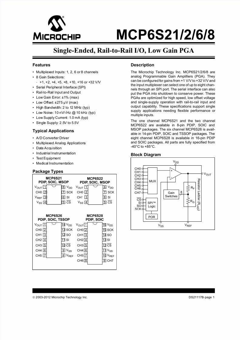
Features
• Multiplexed Inputs: 1, 2, 6 or 8 channels
• 8 Gain Selections:
- +1, +2, +4, +5, +8, +10, +16 or +32 V/V
• Serial Peripheral Interface (SPI)
• Rail-to-Rail Input and Output
• Low Gain Error: ±1% (max)
• Low Offset: ±275 µV (max)
• High Bandwidth: 2 to 12 MHz (typ)
• Low Noise: 10 nV/Hz @ 10 kHz (typ)
• Low Supply Current: 1.0 mA (typ)• Single Supply: 2.5V to 5.5V
Typical Applications
• A/D Converter Driver
• Multiplexed Analog Applications
• Data Acquisition
• Industrial Instrumentation
• Test Equipment
• Medical Instrumentation
Package Types
Description
The Microchip Technology Inc. MCP6S21/2/6/8 are
analog Programmable Gain Amplifiers (PGA). They
can be configured for gains from +1 V/V to +32 V/V and
the input multiplexer can select one of up to eight chan-
nels through an SPI port. The serial interface can also
put the PGA into shutdown to conserve power. These
PGAs are optimized for high speed, low offset voltage
and single-supply operation with rail-to-rail input and
output capability. These specifications support single
supply applications needing flexible performance or
multiple inputs.
The one channel MCP6S21 and the two channel
MCP6S22 are available in 8-pin PDIP, SOIC and
MSOP packages. The six channel MCP6S26 is avail-
able in 14-pin PDIP, SOIC and TSSOP packages. The
eight channel MCP6S28 is available in 16-pin PDIP
and SOIC packages. All parts are fully specified from
-40°C to +85°C.
Block Diagram
VREF
CH0
VSS
SI
SCK
1
2
3
4
8
7
6
5
VDD
CS
VOUT
CH1
CH0
CH2
CS
SI
1
2
3
4
14
13
12
11
VREF
VSS
VOUT
5
6
7
10
9
8
CH3
SCK
VDD
CH5
CH4
CH0
VOUT
CH1
VSS
CS
1
2
3
4
16
15
14
13 SI
SCK
5
6
7
12
11
10
CH2
CH4
CH7
VDD
CH5
8 9
SO
CH6
CH3
SO
CH1
CH0
VSS
SI
SCK
1
2
3
4
8
7
6
5
VDD
CS
VOUT
MCP6S21PDIP, SOIC, MSOP
MCP6S26PDIP, SOIC, TSSOP
MCP6S28PDIP, SOIC
MCP6S22PDIP, SOIC, MSOP
VREF
VOUT
VREF
VDD
CSSI
SOSCK
CH1CH0
CH3
CH2
CH5CH4
CH7
CH6
VSS
8
RF
RG
MUX
SPI™Logic
POR
GainSwitches
+
- R e s i s t or L a d d er ( RL A D )
Single-Ended, Rail-to-Rail I/O, Low Gain PGA
8/10/2019 Mcp6s218 Pga
http://slidepdf.com/reader/full/mcp6s218-pga 2/42
MCP6S21/2/6/8
DS21117B-page 2 2003-2012 Microchip Technology Inc.
1.0 ELECTRICALCHARACTERISTICS
Absolute Maximum Ratings †
VDD - VSS .........................................................................7.0V
All inputs and outputs.. ............... ...... VSS - 0.3V to VDD +0.3V
Difference Input voltage ........................................ |VDD - VSS|
Output Short Circuit Current...................................continuous
Current at Input Pin 2 mA
Current at Output and Supply Pins 30 mA
Storage temperature .............. ................ ....... -65°C to +150°C
Junction temperature ..................................................+150°C
ESD protection on all pins (HBM;MM) 2 kV; 200V
† Notice: Stresses above those listed under "Maximum
Ratings" may cause permanent damage to the device. This is
a stress rating only and functional operation of the device at
those or any other conditions above those indicated in the
operation listings of this specification is not implied. Exposure
to maximum rating conditions for extended periods may affect
device reliability.
PIN FUNCTION TABLE
Name Function
VOUT Analog Output
CH0-CH7 Analog Inputs
VSS Negative Power Supply
VDD Positive Power Supply
SCK SPI Clock Input
SI SPI Serial Data Input
SO SPI Serial Data Output
CS SPI Chip Select
VREF External Reference Pin
DC CHARACTERISTICS
Electrical Specifications: Unless otherwise indicated, T A = +25°C, VDD = +2.5V to +5.5V, VSS = GND, VREF = VSS, G = +1 V/V,
Input = CH0 = (0.3V)/G, CH1 to CH7 = 0.3V, RL = 1 0 k to VDD/2, SI and SCK are tied low and CS is tied high.
Parameters Sym Min Typ Max Units Conditions
Amplifier Input
Input Offset Voltage VOS -275 — +275 µV G = +1, VDD = 4.0V
Input Offset Voltage Drift VOS/T A — ±4 — µV/°C T A = -40 to +85°C
Power Supply Rejection Ratio PSRR 70 85 — dB G = +1 (Note 1)
Input Bias Current IB — ±1 — pA CHx = VDD/2
Input Bias Current over
Temperature
IB — — 250 pA T A = -40 to +85°C,
CHx = VDD/2
Input Impedance ZIN — 1013||15 — ||pF
Input Voltage Range VIVR VSS0.3 — VDD+0.3 V
Amplifier Gain
Nominal Gains — — 1 to 32 — V/V +1, +2, +4, +5, +8, +10, +16 or +32
DC Gain Error G = +1 gE -0.1 — +0.1 % VOUT 0.3V to VDD 0.3V
G +2 gE -1.0 — +1.0 % VOUT 0.3V to VDD 0.3V
DC Gain Drift G = +1 G/T A — ±0.0002 — %/°C T A = -40 to +85°C
G +2 G/T A — ±0.0004 — %/°C T A = -40 to +85°C
Internal Resistance RLAD 3.4 4.9 6.4 k (Note 1)
Internal Resistance over
Temperature
RLAD/T A — +0.028 — %/°C (Note 1)
T A = -40 to +85°C
Amplifier Output
DC Output Non-linearity G = +1 VONL — ±0.003 — % of FSR VOUT = 0.3V to VDD 0.3V, VDD = 5.0V
G +2 VONL — ±0.001 — % of FSR VOUT = 0.3V to VDD 0.3V, VDD = 5.0V
Maximum Output Voltage Swing VOH, VOL VSS+20 — VDD-100 mV G +2; 0.5V output overdrive
VSS+60 — VDD-60 G +2; 0.5V output overdrive,
VREF = VDD/2
Short-Circuit Current IO(SC) — ±30 — mA
Note 1: RLAD (RF + RG in Figure 4-1) connects VREF, VOUT and the inverting input of the internal amplifier. The MCP6S22 has
VREF tied internally to VSS, so VSS is coupled to the internal amplifier and the PSRR spec describes PSRR+ only. We
recommend the MCP6S22’s VSS pin be tied directly to ground to avoid noise problems.
2: IQ includes current in RLAD (typically 60 µA at VOUT = 0.3V). Both IQ and IQ_SHDN exclude digital switching currents.
3: The output goes Hi-Z and the registers reset to their defaults; see Section 5.4, “Power-On Reset”.
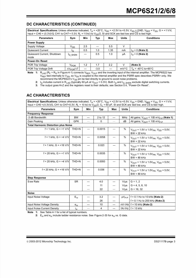
8/10/2019 Mcp6s218 Pga
http://slidepdf.com/reader/full/mcp6s218-pga 3/42
2003-2012 Microchip Technology Inc. DS21117B-page 3
MCP6S21/2/6/8
Power Supply
Supply Voltage VDD 2.5 — 5.5 V
Quiescent Current IQ 0.5 1.0 1.35 mA IO = 0 (Note 2)
Quiescent Current, Shutdown
mode
IQ_SHDN — 0.5 1.0 µA IO = 0 (Note 2)
Power-On Reset
POR Trip Voltage VPOR 1.2 1.7 2.2 V (Note 3)
POR Trip Voltage Drift VPOR/T — -3.0 — mV/°C T A = -40°C to+85°C
DC CHARACTERISTICS (CONTINUED)
Electrical Specifications: Unless otherwise indicated, T A = +25°C, VDD = +2.5V to +5.5V, VSS = GND, VREF = VSS, G = +1 V/V,
Input = CH0 = (0.3V)/G, CH1 to CH7 = 0.3V, RL = 1 0 k to VDD/2, SI and SCK are tied low and CS is tied high.
Parameters Sym Min Typ Max Units Conditions
Note 1: RLAD (RF + RG in Figure 4-1) connects VREF, VOUT and the inverting input of the internal amplifier. The MCP6S22 has
VREF tied internally to VSS, so VSS is coupled to the internal amplifier and the PSRR spec describes PSRR+ only. We
recommend the MCP6S22’s VSS pin be tied directly to ground to avoid noise problems.
2: IQ includes current in RLAD (typically 60 µA at VOUT = 0.3V). Both IQ and IQ_SHDN exclude digital switching currents.
3: The output goes Hi-Z and the registers reset to their defaults; see Section 5.4, “Power-On Reset”.
AC CHARACTERISTICS
Electrical Specifications: Unless otherwise indicated, T A = +25°C, VDD = +2.5V to +5.5V, VSS = GND, VREF = VSS, G = +1 V/V,
Input = CH0 =(0.3V)/G, CH1 to CH7=0.3V, RL = 10 k to VDD/2, CL = 60 pF, SI and SCK are tied low, and CS is tied high.
Parameters Sym Min Typ Max Units Conditions
Frequency Response
-3 dB Bandwidth BW — 2 to 12 — MHz All gains; VOUT < 100 mVP-P (Note 1)
Gain Peaking GPK — 0 — dB All gains; VOUT < 100 mVP-P
Total Harmonic Distortion plus Noise
f = 1 kHz, G = +1 V/V THD+N — 0.0015 — % VOUT = 1.5V ± 1.0VPK, VDD = 5.0V,
BW = 22 kHz
f = 1 kHz, G = +4 V/V THD+N — 0.0058 — % VOUT = 1.5V ± 1.0VPK, VDD = 5.0V,
BW = 22 kHz
f = 1 kHz, G = +16 V/V THD+N — 0.023 — % VOUT = 1.5V ± 1.0VPK, VDD = 5.0V,BW = 22 kHz
f = 20 kHz, G = +1 V/V THD+N — 0.0035 — % VOUT = 1.5V ± 1.0VPK, VDD = 5.0V,
BW = 80 kHz
f = 20 kHz, G = +4 V/V THD+N — 0.0093 — % VOUT = 1.5V ± 1.0VPK, VDD = 5.0V,
BW = 80 kHz
f = 20 kHz, G = +16 V/V THD+N — 0.036 — % VOUT = 1.5V ± 1.0VPK, VDD = 5.0V,
BW = 80 kHz
Step Response
Slew Rate SR — 4.0 — V/µs G = 1, 2
— 11 — V/µs G = 4, 5, 8, 10
— 22 — V/µs G = 16, 32
Noise
Input Noise Voltage Eni — 3.2 — µVP-P f = 0.1 Hz to 10 kHz (Note 2)
— 26 — f = 0.1 Hz to 200 kHz (Note 2)
Input Noise Voltage Density eni — 10 — nV/Hz f = 10 kHz (Note 2)
Input Noise Current Density ini — 4 — fA/Hz f = 10 kHz
Note 1: See Table 4-1 for a list of typical numbers.
2: Eni and eni include ladder resistance noise. See Figure 2-33 for eni vs. G data.
8/10/2019 Mcp6s218 Pga
http://slidepdf.com/reader/full/mcp6s218-pga 4/42
MCP6S21/2/6/8
DS21117B-page 4 2003-2012 Microchip Technology Inc.
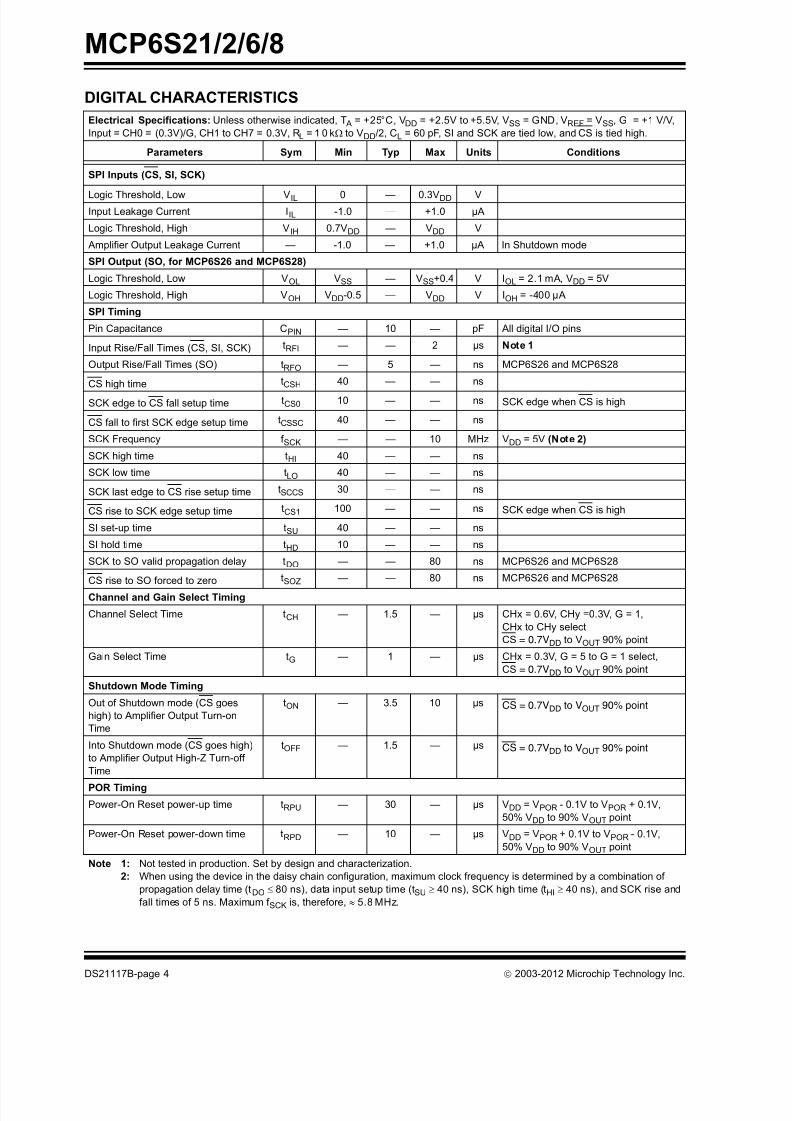
DIGITAL CHARACTERISTICS
Electrical Specifications: Unless otherwise indicated, T A = +25°C, VDD = +2.5V to +5.5V, VSS = GND, VREF = VSS, G = +1 V/V,
Input = CH0 = (0.3V)/G, CH1 to CH7 = 0.3V, RL = 1 0 k to VDD/2, CL = 60 pF, SI and SCK are tied low, and CS is tied high.
Parameters Sym Min Typ Max Units Conditions
SPI Inputs (CS, SI, SCK)
Logic Threshold, Low VIL 0 — 0.3VDD VInput Leakage Current IIL -1.0 — +1.0 µA
Logic Threshold, High VIH 0.7VDD — VDD V
Amplifier Output Leakage Current — -1.0 — +1.0 µA In Shutdown mode
SPI Output (SO, for MCP6S26 and MCP6S28)
Logic Threshold, Low VOL VSS — VSS+0.4 V IOL = 2.1 mA, VDD = 5V
Logic Threshold, High VOH VDD-0.5 — VDD V IOH = -400 µA
SPI Timing
Pin Capacitance CPIN — 10 — pF All digital I/O pins
Input Rise/Fall Times (CS, SI, SCK) tRFI — — 2 µs Note 1
Output Rise/Fall Times (SO) tRFO — 5 — ns MCP6S26 and MCP6S28
CS high time tCSH 40 — — ns
SCK edge to CS fall setup time tCS0 10 — — ns SCK edge when CS is high
CS fall to first SCK edge setup time tCSSC 40 — — ns
SCK Frequency f SCK — — 10 MHz VDD = 5V (Note 2)
SCK high time tHI 40 — — ns
SCK low time tLO 40 — — ns
SCK last edge to CS rise setup time tSCCS 30 — — ns
CS rise to SCK edge setup time tCS1 100 — — ns SCK edge when CS is high
SI set-up time tSU 40 — — ns
SI hold time tHD 10 — — ns
SCK to SO valid propagation delay tDO — — 80 ns MCP6S26 and MCP6S28
CS rise to SO forced to zero tSOZ — — 80 ns MCP6S26 and MCP6S28
Channel and Gain Select Timing
Channel Select Time tCH — 1.5 — µs CHx = 0.6V, CHy =0.3V, G = 1,
CHx to CHy select
CS = 0.7VDD to VOUT 90% point
Gain Select Time tG — 1 — µs CHx = 0.3V, G = 5 to G = 1 select,
CS = 0.7VDD to VOUT 90% point
Shutdown Mode Timing
Out of Shutdown mode (CS goes
high) to Amplifier Output Turn-on
Time
tON — 3.5 10 µs CS = 0.7VDD to VOUT 90% point
Into Shutdown mode (CS goes high)
to Amplifier Output High-Z Turn-off
Time
tOFF — 1.5 — µs CS = 0.7VDD to VOUT 90% point
POR Timing
Power-On Reset power-up time tRPU — 30 — µs VDD = VPOR - 0.1V to VPOR + 0.1V,
50% VDD to 90% VOUT point
Power-On Reset power-down time tRPD — 10 — µs VDD = VPOR + 0.1V to VPOR - 0.1V,
50% VDD to 90% VOUT point
Note 1: Not tested in production. Set by design and characterization.
2: When using the device in the daisy chain configuration, maximum clock frequency is determined by a combination of
propagation delay time (tDO 80 ns), data input setup time (tSU 40 ns), SCK high time (tHI 40 ns), and SCK rise and
fall times of 5 ns. Maximum f SCK is, therefore, 5.8 MHz.
8/10/2019 Mcp6s218 Pga
http://slidepdf.com/reader/full/mcp6s218-pga 5/42
2003-2012 Microchip Technology Inc. DS21117B-page 5
MCP6S21/2/6/8
TEMPERATURE CHARACTERISTICS
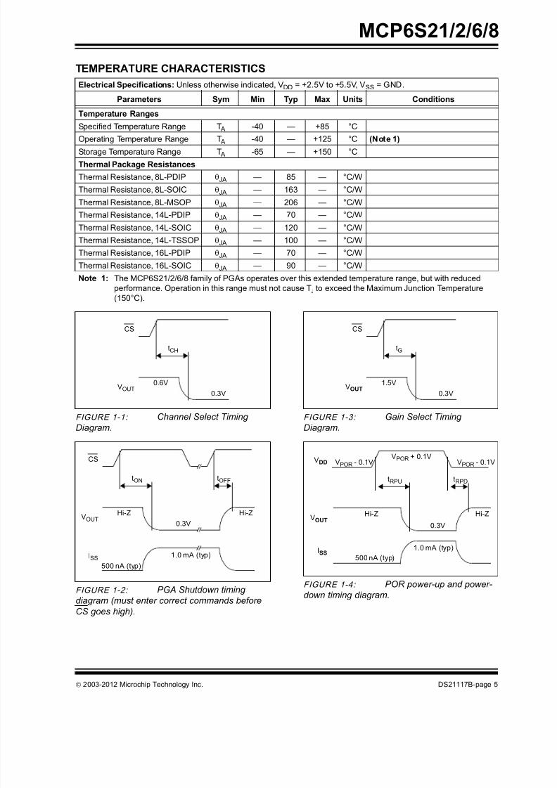
FIGURE 1-1: Channel Select TimingDiagram.
FIGURE 1-2: PGA Shutdown timing
diagram (must enter correct commands before
CS goes high).
FIGURE 1-3: Gain Select TimingDiagram.
FIGURE 1-4: POR power-up and power-
down timing diagram.
Electrical Specifications: Unless otherwise indicated, VDD = +2.5V to +5.5V, VSS = GND.
Parameters Sym Min Typ Max Units Conditions
Temperature Ranges
Specified Temperature Range T A -40 — +85 °C
Operating Temperature Range T A -40 — +125 °C (Note 1)
Storage Temperature Range T A -65 — +150 °C
Thermal Package Resistances
Thermal Resistance, 8L-PDIP JA — 85 — °C/W
Thermal Resistance, 8L-SOIC JA — 163 — °C/W
Thermal Resistance, 8L-MSOP JA — 206 — °C/W
Thermal Resistance, 14L-PDIP JA — 70 — °C/W
Thermal Resistance, 14L-SOIC JA — 120 — °C/W
Thermal Resistance, 14L-TSSOP JA — 100 — °C/W
Thermal Resistance, 16L-PDIP JA — 70 — °C/W
Thermal Resistance, 16L-SOIC JA — 90 — °C/W
Note 1: The MCP6S21/2/6/8 family of PGAs operates over this extended temperature range, but with reducedperformance. Operation in this range must not cause TJ to exceed the Maximum Junction Temperature
(150°C).
CS
VOUT
tCH
0.6V
0.3V
CS
tOFF
VOUT
tON
Hi-Z Hi-Z
ISS
500 nA (typ)
1.0 mA (typ)
0.3V
CS
VOUT
tG
1.5V
0.3V
VDD
tRPD
VOUT
tRPU
Hi-Z Hi-Z
VPOR - 0.1V VPOR - 0.1VVPOR + 0.1V
0.3V
ISS500 nA (typ)
1.0 mA (typ)
8/10/2019 Mcp6s218 Pga
http://slidepdf.com/reader/full/mcp6s218-pga 6/42
MCP6S21/2/6/8
DS21117B-page 6 2003-2012 Microchip Technology Inc.
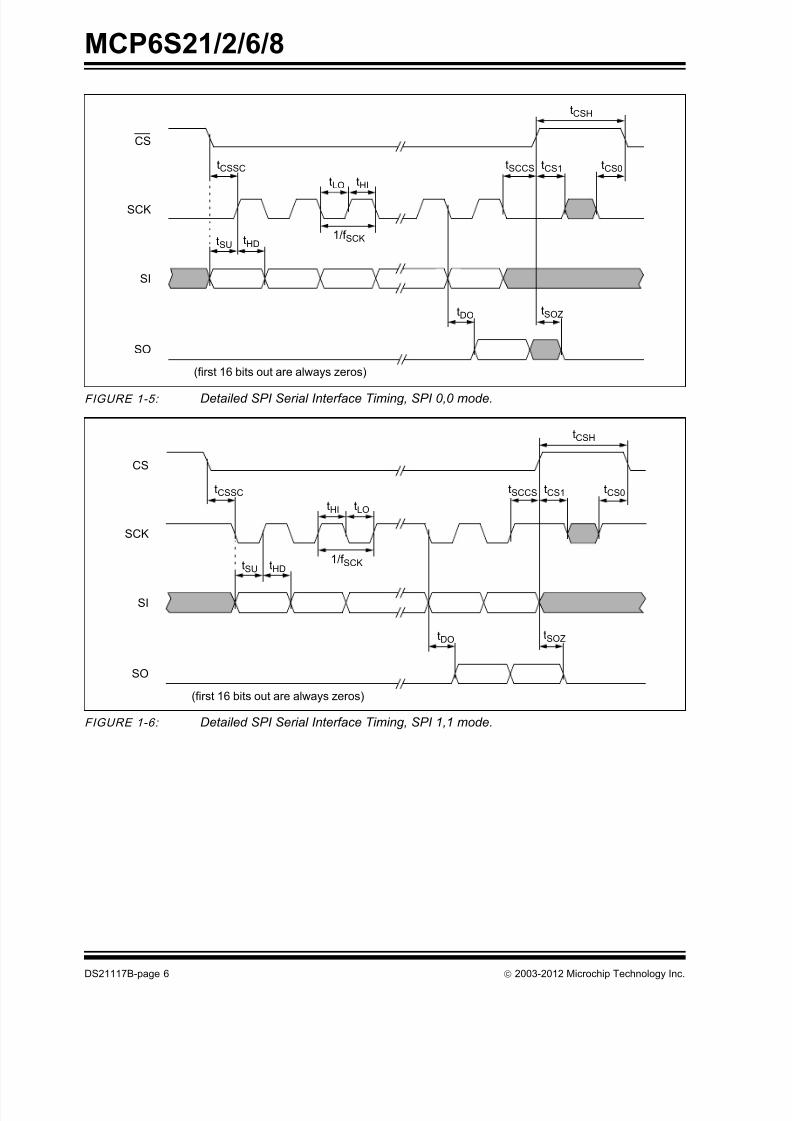
FIGURE 1-5: Detailed SPI Serial Interface Timing, SPI 0,0 mode.
FIGURE 1-6: Detailed SPI Serial Interface Timing, SPI 1,1 mode.
CS
SCK
SI
tSU tHD
tCSSC tSCCS
tCSH
SO
(first 16 bits out are always zeros)
tDO tSOZ
tLO tHI
1/f SCK
tCS0tCS1
CS
SCK
SI
tSU tHD
tCSSC tSCCS
SO
(first 16 bits out are always zeros)
tDO tSOZ
tHI tLO
1/f SCK
tCS1
tCSH
tCS0
8/10/2019 Mcp6s218 Pga
http://slidepdf.com/reader/full/mcp6s218-pga 7/42
2003-2012 Microchip Technology Inc. DS21117B-page 7
MCP6S21/2/6/8
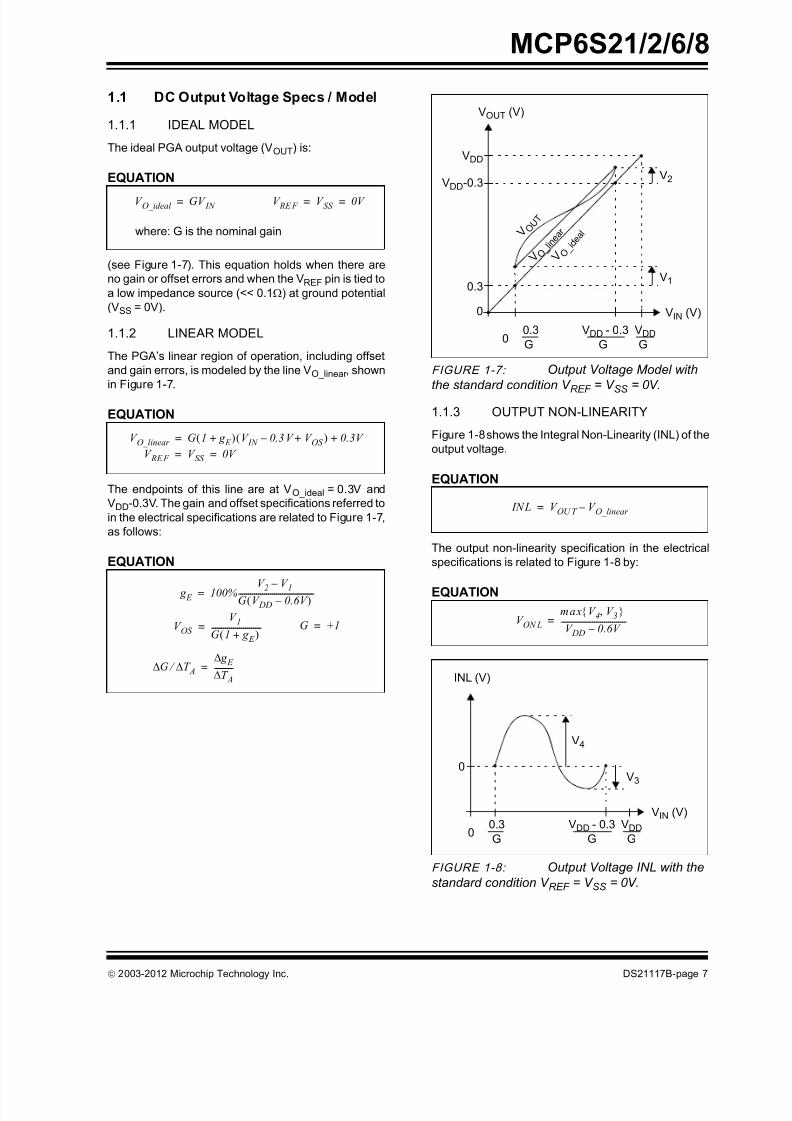
1.1 DC Output Voltage Specs / Model
1.1.1 IDEAL MODEL
The ideal PGA output voltage (VOUT) is:
EQUATION
(see Figure 1-7). This equation holds when there are
no gain or offset errors and when the VREF pin is tied to
a low impedance source (<< 0.1) at ground potential
(VSS = 0V).
1.1.2 LINEAR MODEL
The PGA’s linear region of operation, including offset
and gain errors, is modeled by the line VO_linear , shown
in Figure 1-7.
EQUATION
The endpoints of this line are at VO_ideal = 0.3V and
VDD-0.3V. The gain and offset specifications referred to
in the electrical specifications are related to Figure 1-7,
as follows:
EQUATION
FIGURE 1-7: Output Voltage Model with
the standard condition V REF
= V SS
= 0V.
1.1.3 OUTPUT NON-LINEARITY
Figure 1-8 shows the Integral Non-Linearity (INL) of the
output voltage.
EQUATION
The output non-linearity specification in the electrical
specifications is related to Figure 1-8 by:
EQUATION
FIGURE 1-8: Output Voltage INL with the
standard condition V REF = V SS = 0V.
V O_ideal GV IN = V RE F V SS 0V = =
where: G is the nominal gain
V O_linear G 1 g E + V IN 0.3V V OS +– 0.3V +=
V RE F V SS 0V = =
g E 100% V 2 V 1–
G V DD 0.6V – --------------------------------------
=
V OS
V 1
G 1 g E + -------------------------=
G T A g E
T A----------=
G +1=
0
0
0.3
VDD-0.3
VDD
V O U T
VOUT (V)
VIN (V)
0.3 VDD - 0.3 VDD
GG G
V1
V O_ i d e a l
V O_ l i n e a
r
V2
INL V OU T V O_linear –=
V ON L
max V 4 V 3
V DD 0.6V –
---------------------------------=
0V3
V4
INL (V)
VIN (V)0.3 VDD - 0.3 VDD
GG G0
8/10/2019 Mcp6s218 Pga
http://slidepdf.com/reader/full/mcp6s218-pga 8/42
MCP6S21/2/6/8
DS21117B-page 8 2003-2012 Microchip Technology Inc.
1.1.4 DIFFERENT VREF CONDITIONS
Some of the plots in Section 2.0, “Typical Performance
Curves”, have the conditions VREF = VDD/2 or
VREF = VDD. The equations and figures above are eas-
ily modified for these conditions. The ideal VOUT
becomes:
EQUATION
The complete linear model is:
EQUATION
where the new VIN endpoints are:
EQUATION
The equations for extracting the specifications do not
change.
V O_ideal V RE F G V IN V RE F – +=
V DD V RE F V SS 0V =
V O_linear G 1 g E + V IN V IN_L V OS +– 0.3V +=
V IN_L
0.3V V RE F –
G V RE F +
------------------------------=
V IN_R
V DD 0.3V – V RE F –
G V RE F +
-----------------------------------------------=

8/10/2019 Mcp6s218 Pga
http://slidepdf.com/reader/full/mcp6s218-pga 9/42
2003-2012 Microchip Technology Inc. DS21117B-page 9
MCP6S21/2/6/8
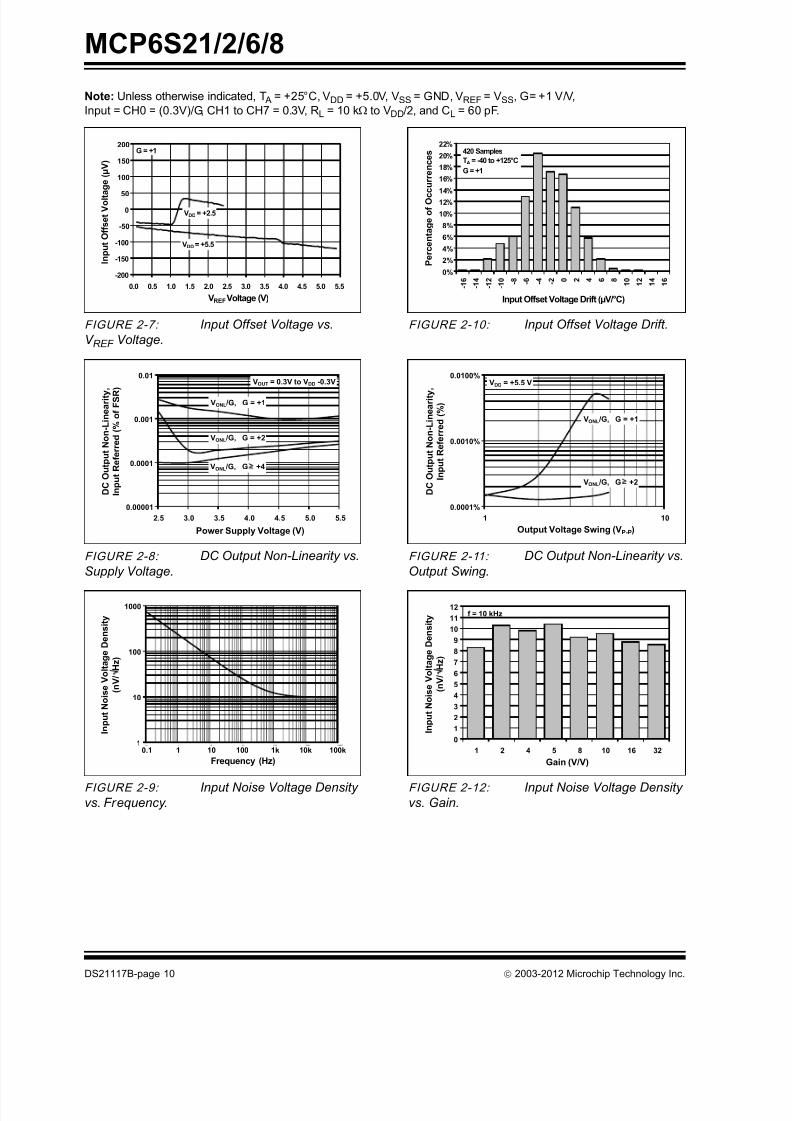
2.0 TYPICAL PERFORMANCE CURVES
Note: Unless otherwise indicated, T A
= +25°C, VDD
= +5.0V, VSS
= GND, VREF
= VSS
, G= +1 V/V,
Input = CH0 = (0.3V)/G, CH1 to CH7 = 0.3V, RL = 10 k to VDD/2, and CL = 60 pF.
FIGURE 2-1: DC Gain Error, G = +1.
FIGURE 2-2: DC Gain Error, G +2.
FIGURE 2-3: Ladder Resistance Drift.
FIGURE 2-4: DC Gain Drift, G = +1.
FIGURE 2-5: DC Gain Drift, G +2.
FIGURE 2-6: Input Offset Voltage,
V DD = 4.0V.
Note: The graphs and tables provided following this note are a statistical summary based on a limited number of
samples and are provided for informational purposes only. The performance characteristics listed herein
are not tested or guaranteed. In some graphs or tables, the data presented may be outside the specified
operating range (e.g., outside specified power supply range) and therefore outside the warranted range.
0%
2%
4%
6%
8%
10%
12%
14%
16%
18%
20%
22%
- 0 . 0 4 0
- 0 . 0 3 6
- 0 . 0 3 2
- 0 . 0 2 8
- 0 . 0 2 4
- 0 . 0 2 0
- 0 . 0 1 6
- 0 . 0 1 2
- 0 . 0 0 8
- 0 . 0 0 4
0 . 0 0 0
0 . 0 0 4
DC Gain Error (%)
P e r c e n t a g e o f O c c u r r e n c e s
420 Samples
G = +1
0%
2%
4%
6%
8%
10%
12%
14%
16%
18%
- 0 . 5
- 0 . 4
- 0 . 3
- 0 . 2
- 0 . 1
0 . 0
0 . 1
0 . 2
0 . 3
0 . 4
0 . 5
DC Gain Error (%)
P e r c e n t a g e o f O c c u r r e n c e s 420 Samples
G +2
0%
2%
4%
6%
8%
10%
12%
14%
16%
18%
20%
22%
0 . 0 2 3
0 . 0 2 4
0 . 0 2 5
0 . 0 2 6
0 . 0 2 7
0 . 0 2 8
0 . 0 2 9
0 . 0 3 0
0 . 0 3 1
Ladder Resistance Drift (%/°C)
P
e r c e n t a g e o f O c c u r r e n c e s 420 Samples
TA = -40 to +125°C
0%
2%
4%
6%
8%
10%
12%
14%
16%
18%
- 0 . 0 0 0 6
- 0 . 0 0 0 5
- 0 . 0 0 0 4
- 0 . 0 0 0 3
- 0 . 0 0 0 2
- 0 . 0 0 0 1
0 . 0 0 0 0
0 . 0 0 0 1
0 . 0 0 0 2
0 . 0 0 0 3
0 . 0 0 0 4
0 . 0 0 0 5
0 . 0 0 0 6
DC Gain Drift (%/°C)
P e r c e n t a g e o f O c c u r r e n c e s
420 Samples
G = +1TA = -40 to +125°C
0%
2%
4%
6%
8%
10%
12%
14%
16%
18%
20%
22%
24%
- 0 . 0 0 2 0
- 0 . 0 0 1 6
- 0 . 0 0 1 2
- 0 . 0 0 0 8
- 0 . 0 0 0 4
0 . 0 0 0 0
0 . 0 0 0 4
0 . 0 0 0 8
0 . 0 0 1 2
0 . 0 0 1 6
0 . 0 0 2 0
DC Gain Drift (%/°C)
P e r c e n t a g e o f O c c u r r e n c e s
420 Samples
G +2TA = -40 to +125°C
0%
2%
4%
6%
8%
10%
12%
14%
16%
18%
20%
- 2 4 0
- 2 0 0
- 1 6 0
- 1 2 0
- 8 0
- 4 0 0
4 0
8 0
1 2 0
1 6 0
2 0 0
2 4 0
Input Offset Voltage (µV)
P e r c e n t a g e o f O c c u r r e n c e s 360 Samples
VDD = 4.0 V
G = +1
8/10/2019 Mcp6s218 Pga
http://slidepdf.com/reader/full/mcp6s218-pga 10/42
MCP6S21/2/6/8
DS21117B-page 10 2003-2012 Microchip Technology Inc.
Note: Unless otherwise indicated, T A = +25°C, VDD = +5.0V, VSS = GND, VREF = VSS, G= +1 V/V,
Input = CH0 = (0.3V)/G, CH1 to CH7 = 0.3V, RL = 10 k to VDD/2, and CL = 60 pF.
FIGURE 2-7: Input Offset Voltage vs.
V REF Voltage.
FIGURE 2-8: DC Output Non-Linearity vs.
Supply Voltage.
FIGURE 2-9: Input Noise Voltage Densityvs. Frequency.
FIGURE 2-10: Input Offset Voltage Drift.
FIGURE 2-11: DC Output Non-Linearity vs.
Output Swing.
FIGURE 2-12: Input Noise Voltage Densityvs. Gain.
-200
-150
-100
-50
0
50
100
150
200
0.0 0.5 1.0 1.5 2.0 2.5 3.0 3.5 4.0 4.5 5.0 5.5
VREF Voltage (V)
I n p u t O f f s e t V o l t a g e ( µ V )
VDD = +5.5
VDD = +2.5
G = +1
0.00001
0.0001
0.001
0.01
2.5 3.0 3.5 4.0 4.5 5.0 5.5
Power Supply Voltage (V)
D C O u t p u t N o n - L i n e a r i t y
,
I n p u t R e f e r r e d ( % o
f F S R
)
VONL /G, G = +1
VONL /G, G = +2
VONL /G, G +4
VOUT = 0.3V to VDD -0.3V
1
10
100
1000
0.1 1 10 100 1000 10000 100000
Frequency (Hz)
I n p u t N o i s e V o l t a g e D e n s i t y
( n V / H z )
1k 10k 100k1 10 1000.1
0%
2%
4%
6%
8%
10%
12%
14%
16%
18%
20%
22%
- 1 6
- 1 4
- 1 2
- 1 0 - 8 - 6 - 4 - 2 0 2 4 6 8
1 0
1 2
1 4
1 6
Input Offset Voltage Drift (µV/°C)
P e r c e n t a g e o f O c
c u r r e n c e s 420 Samples
TA = -40 to +125°C
G = +1
0.0001%
0.0010%
0.0100%
1 10
Output Voltage Swing (VP-P)
D C O u t p u t N o n - L i n e a r i t y
,
I n p u t R e f e r r e d ( % )
VONL /G, G +2
VONL /G, G = +1
VDD = +5.5 V
0
1
2
3
4
5
6
7
8
9
10
11
12
1 2 4 5 8 10 16 32
Gain (V/V)
I n p u t N o i s e V o l t a g e D e n s i t y
( n V / H z )
f = 10 kHz
8/10/2019 Mcp6s218 Pga
http://slidepdf.com/reader/full/mcp6s218-pga 11/42
2003-2012 Microchip Technology Inc. DS21117B-page 11
MCP6S21/2/6/8
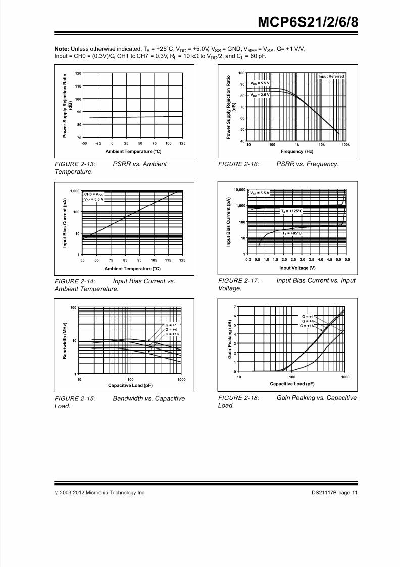
Note: Unless otherwise indicated, T A = +25°C, VDD = +5.0V, VSS = GND, VREF = VSS, G= +1 V/V,
Input = CH0 = (0.3V)/G, CH1 to CH7 = 0.3V, RL = 10 k to VDD/2, and CL = 60 pF.
FIGURE 2-13: PSRR vs. Ambient
Temperature.
FIGURE 2-14: Input Bias Current vs.
Ambient Temperature.
FIGURE 2-15: Bandwidth vs. CapacitiveLoad.
FIGURE 2-16: PSRR vs. Frequency.
FIGURE 2-17: Input Bias Current vs. Input
Voltage.
FIGURE 2-18: Gain Peaking vs. CapacitiveLoad.
70
80
90
100
110
120
-50 -25 0 25 50 75 100 125
Ambient Temperature (°C)
P o w e r S u p p l y R e j e
c t i o n R a t i o
( d B )
1
10
100
1,000
55 65 75 85 95 105 115 125
Ambient Temperature (°C)
I n p u t B i a s C u r r e n t ( p A )
CH0 = VDD
VDD = 5.5 V
1
10
100
10 100 1000
Capacitive Load (pF)
B a n d w i d t h ( M H z )
G = +1
G = +4
G = +16
40
50
60
70
80
90
100
10 100 10 00 1 0000 100000
Frequency (Hz)
P o w e r S u p p l y R e j e c t i o n R a t i o
( d B )
VDD = 2.5 V
VDD = 5.5 V
1k 10k 100k10 100
Input Referred
1
10
100
1,000
10,000
0.0 0.5 1.0 1.5 2.0 2.5 3.0 3.5 4.0 4.5 5.0 5.5
Input Voltage (V)
I n p u t B i a s C u r r e n t ( p A )
TA = +85°C
VDD = 5.5 V
TA = +125°C
0
1
2
3
4
5
6
7
10 100 1000
Capacitive Load (pF)
G a i n P e a k i n g ( d B )
G = +1
G = +4
G = +16
8/10/2019 Mcp6s218 Pga
http://slidepdf.com/reader/full/mcp6s218-pga 12/42
MCP6S21/2/6/8
DS21117B-page 12 2003-2012 Microchip Technology Inc.
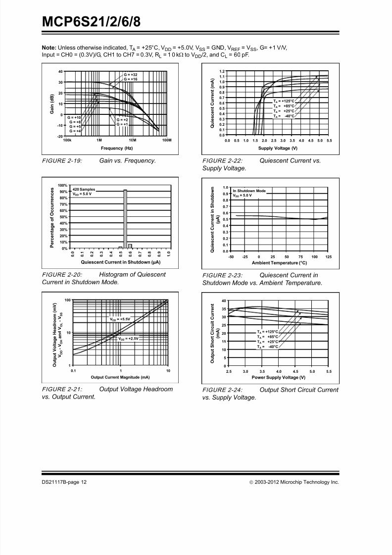
Note: Unless otherwise indicated, T A = +25°C, VDD = +5.0V, VSS = GND, VREF = VSS, G= +1 V/V,
Input = CH0 = (0.3V)/G, CH1 to CH7 = 0.3V, RL = 1 0 k to VDD/2, and CL = 60 pF.
FIGURE 2-19: Gain vs. Frequency.
FIGURE 2-20: Histogram of Quiescent
Current in Shutdown Mode.
FIGURE 2-21: Output Voltage Headroomvs. Output Current.
FIGURE 2-22: Quiescent Current vs.
Supply Voltage.
FIGURE 2-23: Quiescent Current in
Shutdown Mode vs. Ambient Temperature.
FIGURE 2-24: Output Short Circuit Currentvs. Supply Voltage.
-20
-10
0
10
20
30
40
1.E+05 1.E+06 1.E+07 1.E+08
Frequency (Hz)
G a i n ( d B
)
G = +2
G = +1
1M 10M 100M100k
G = +32
G = +16
G = +10
G = +8
G = +5
G = +4
0%
10%
20%
30%
40%
50%
60%
70%
80%
90%
100%
0 . 0
0 . 1
0 . 2
0 . 3
0 . 4
0 . 5
0 . 6
0 . 7
0 . 8
0 . 9
1 . 0
Quiescent Current in Shutdown (µA)
P e r c e n t a g e o f O c c u r r e n c
e s 420 Samples
VDD = 5.0 V
1
10
100
0.1 1 10
Output Current Magnitude (mA)
O u t p u t V o l t a g e H e a d r o o m ( m V )
V D D - V O H a n d V O L - V S S
VDD = +5.5V
VDD = +2.5V
0.0
0.1
0.2
0.3
0.4
0.5
0.6
0.7
0.8
0.9
1.0
1.1
1.2
0.0 0.5 1.0 1.5 2.0 2.5 3.0 3.5 4.0 4.5 5.0 5.5
Supply Voltage (V)
Q u i e s c e n t C u r r e n t ( m A )
TA = +125°C
TA = +85°C
TA = +25°C
TA = -40°C
0.0
0.1
0.2
0.3
0.4
0.5
0.6
0.7
0.80.9
1.0
-50 -25 0 25 50 75 100 125
Ambient Temperature (°C)
Q u i e s c e n t C u r r e n t i n S h u t d o
w n
( µ A )
In Shutdown Mode
VDD = 5.0 V
0
5
10
15
20
25
30
35
40
2.5 3.0 3.5 4.0 4.5 5.0 5.5
Power Supply Voltage (V)
O u t p u t S h o r t C i r c u i t C u r r e n t
( m A )
TA = +125°C
TA = +85°C
TA = +25°C
TA = -40°C
8/10/2019 Mcp6s218 Pga
http://slidepdf.com/reader/full/mcp6s218-pga 13/42
8/10/2019 Mcp6s218 Pga
http://slidepdf.com/reader/full/mcp6s218-pga 14/42
MCP6S21/2/6/8
DS21117B-page 14 2003-2012 Microchip Technology Inc.
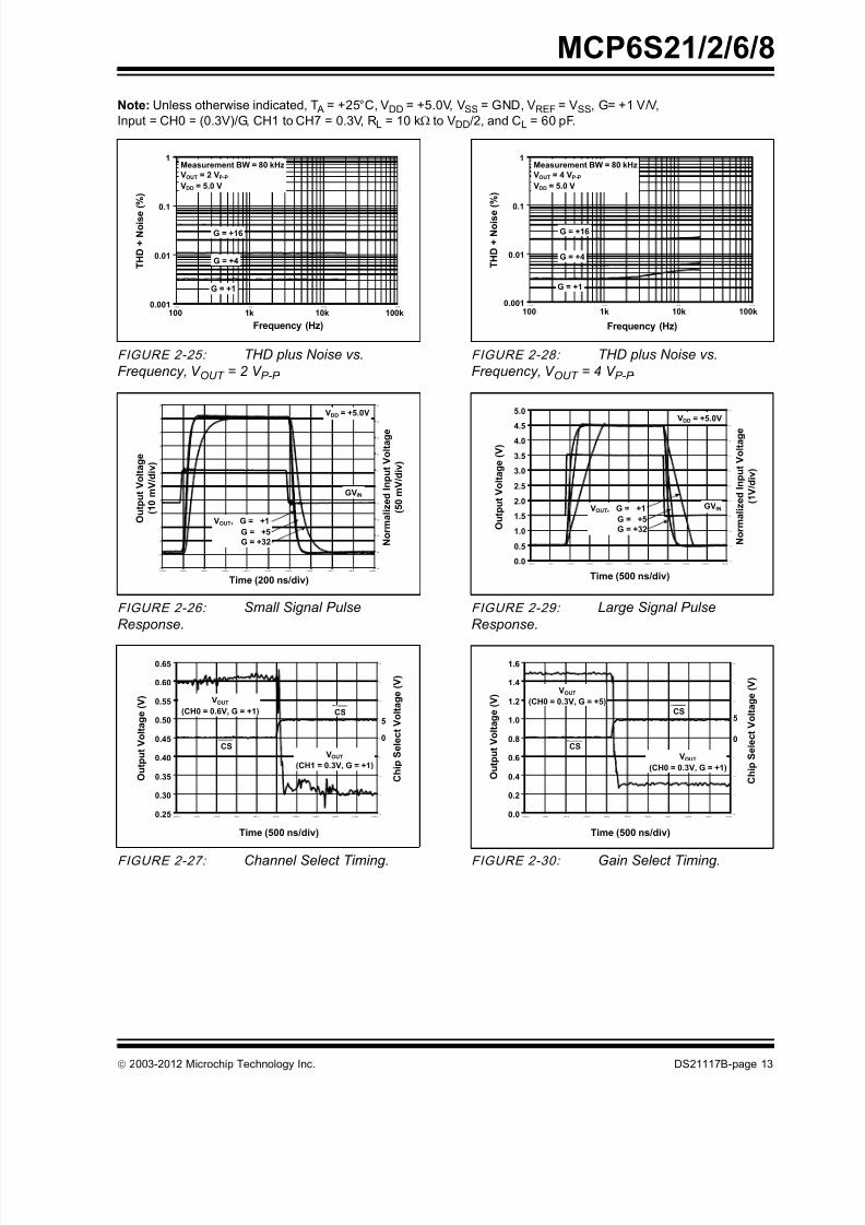
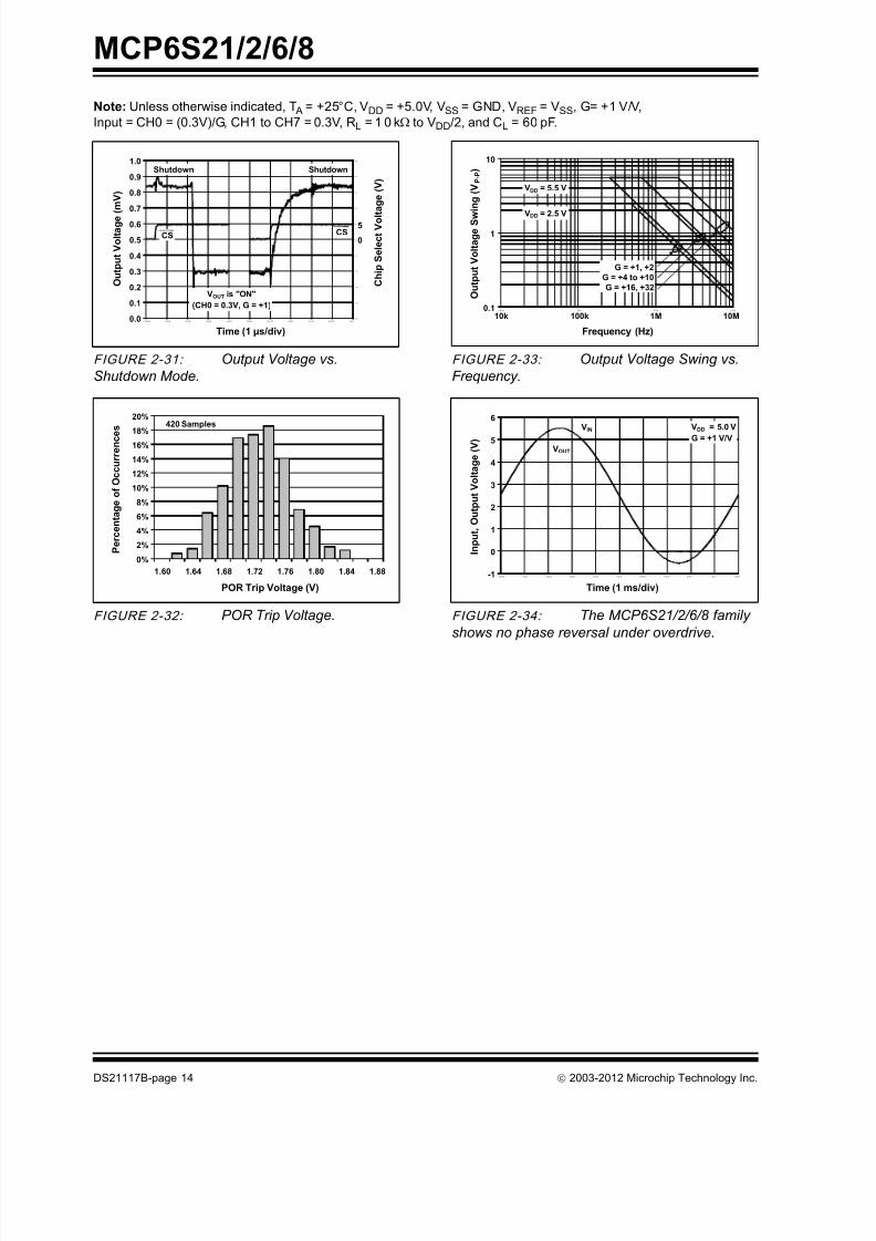
Note: Unless otherwise indicated, T A = +25°C, VDD = +5.0V, VSS = GND, VREF = VSS, G= +1 V/V,
Input = CH0 = (0.3V)/G, CH1 to CH7 = 0.3V, RL = 1 0 k to VDD/2, and CL = 60 pF.
FIGURE 2-31: Output Voltage vs.
Shutdown Mode.
FIGURE 2-32: POR Trip Voltage.
FIGURE 2-33: Output Voltage Swing vs.
Frequency.
FIGURE 2-34: The MCP6S21/2/6/8 family
shows no phase reversal under overdrive.
0.0
0.1
0.2
0.3
0.4
0.5
0.6
0.7
0.8
0.9
1.0
0.0E+00 1.0E-06 2.0 E-06 3.0 E-06 4.0E-0 6 5.0E-06 6.0E-06 7.0E-06 8.0E-0 6 9.0E-06 1.0E -05
Time (1 µs/div)
O u t p u t V o l t a g e
( m V )
-25
-20
-15
-10
-5
0
5
10
15
20
25
C h i p S e l e c t V o l t a g e ( V )
5
0
VOUT is "ON"
(CH0 = 0.3V, G = +1)
Shutdown
CSCS
Shutdown
0%
2%
4%
6%
8%
10%
12%
14%
16%18%
20%
1.60 1.64 1.68 1.72 1.76 1.80 1.84 1.88
POR Trip Voltage (V)
P e r c e n t a g e o f O c c u r r e n c e
s 420 Samples
0.1
1
10
1.E+04 1.E+05 1.E+06 1.E+07
Frequency (Hz)
O u t p u t V o l t a g e S w
i n g ( V P - P )
VDD = 2.5 V
VDD = 5.5 V
G = +1, +2
G = +4 to +10
G = +16, +32
10k 100k 10M1M
-1
0
1
2
3
4
5
6
0.0E+00 1.0E-0 3 2.0E-03 3.0E-03 4.0E-03 5.0E-03 6 .0E-03 7.0E-03 8.0E -03 9.0E -03 1.0E-02
Time (1 ms/div)
I n p u t , O u t p u t V o l t a g e ( V )
VDD = 5.0 V
G = +1 V/V
VIN
VOUT
8/10/2019 Mcp6s218 Pga
http://slidepdf.com/reader/full/mcp6s218-pga 15/42
2003-2012 Microchip Technology Inc. DS21117B-page 15
MCP6S21/2/6/8
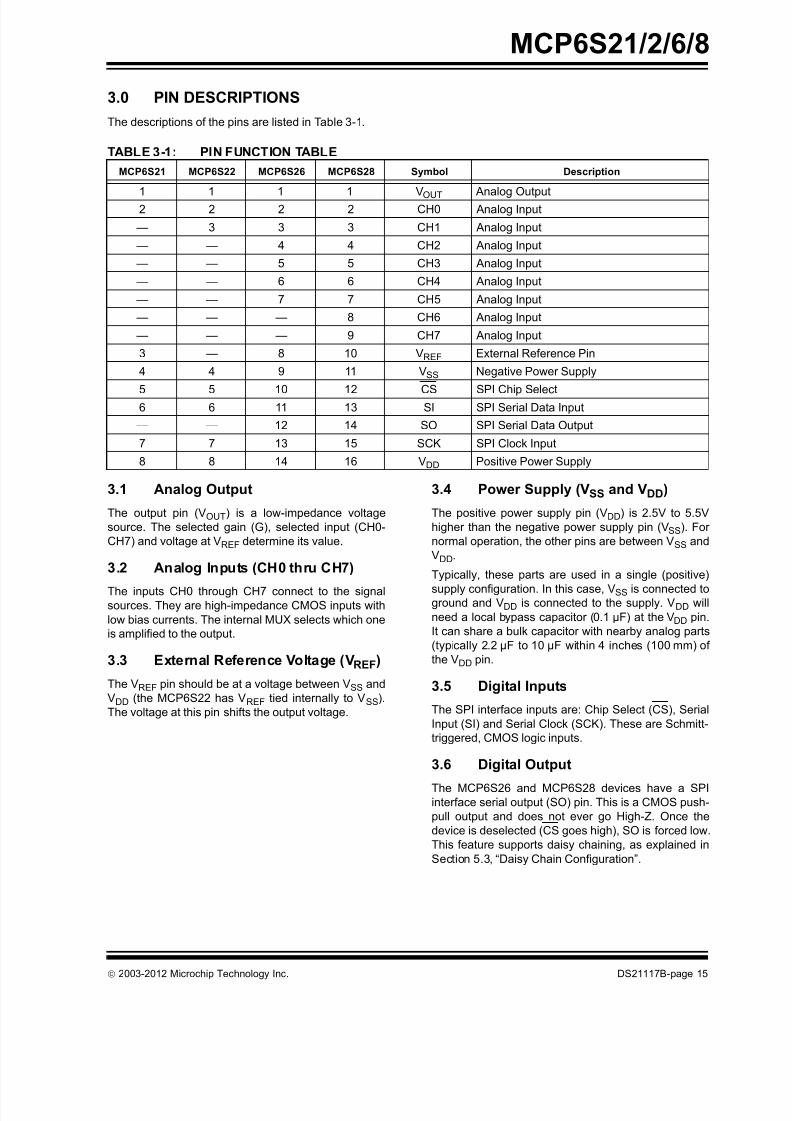
3.0 PIN DESCRIPTIONS
The descriptions of the pins are listed in Table 3-1.
TABLE 3-1: PIN FUNCTION TABLE
3.1 Analog Output
The output pin (VOUT) is a low-impedance voltage
source. The selected gain (G), selected input (CH0-
CH7) and voltage at VREF determine its value.
3.2 Analog Inputs (CH0 thru CH7)
The inputs CH0 through CH7 connect to the signalsources. They are high-impedance CMOS inputs with
low bias currents. The internal MUX selects which one
is amplified to the output.
3.3 External Reference Voltage (VREF)
The VREF pin should be at a voltage between VSS and
VDD (the MCP6S22 has VREF tied internally to VSS).
The voltage at this pin shifts the output voltage.
3.4 Power Supply (VSS and VDD)
The positive power supply pin (VDD) is 2.5V to 5.5V
higher than the negative power supply pin (VSS). For
normal operation, the other pins are between VSS and
VDD.
Typically, these parts are used in a single (positive)
supply configuration. In this case, VSS is connected toground and VDD is connected to the supply. VDD will
need a local bypass capacitor (0.1 µF) at the VDD pin.
It can share a bulk capacitor with nearby analog parts
(typically 2.2 µF to 10 µF within 4 inches (100 mm) of
the VDD pin.
3.5 Digital Inputs
The SPI interface inputs are: Chip Select (CS), Serial
Input (SI) and Serial Clock (SCK). These are Schmitt-
triggered, CMOS logic inputs.
3.6 Digital Output
The MCP6S26 and MCP6S28 devices have a SPIinterface serial output (SO) pin. This is a CMOS push-
pull output and does not ever go High-Z. Once the
device is deselected (CS goes high), SO is forced low.
This feature supports daisy chaining, as explained in
Section 5.3, “Daisy Chain Configuration”.
MCP6S21 MCP6S22 MCP6S26 MCP6S28 Symbol Description
1 1 1 1 VOUT Analog Output2 2 2 2 CH0 Analog Input
— 3 3 3 CH1 Analog Input
— — 4 4 CH2 Analog Input
— — 5 5 CH3 Analog Input
— — 6 6 CH4 Analog Input
— — 7 7 CH5 Analog Input
— — — 8 CH6 Analog Input
— — — 9 CH7 Analog Input
3 — 8 10 VREF External Reference Pin
4 4 9 11 VSS Negative Power Supply
5 5 10 12 CS SPI Chip Select6 6 11 13 SI SPI Serial Data Input
— — 12 14 SO SPI Serial Data Output
7 7 13 15 SCK SPI Clock Input
8 8 14 16 VDD Positive Power Supply
8/10/2019 Mcp6s218 Pga
http://slidepdf.com/reader/full/mcp6s218-pga 16/42
MCP6S21/2/6/8
DS21117B-page 16 2003-2012 Microchip Technology Inc.
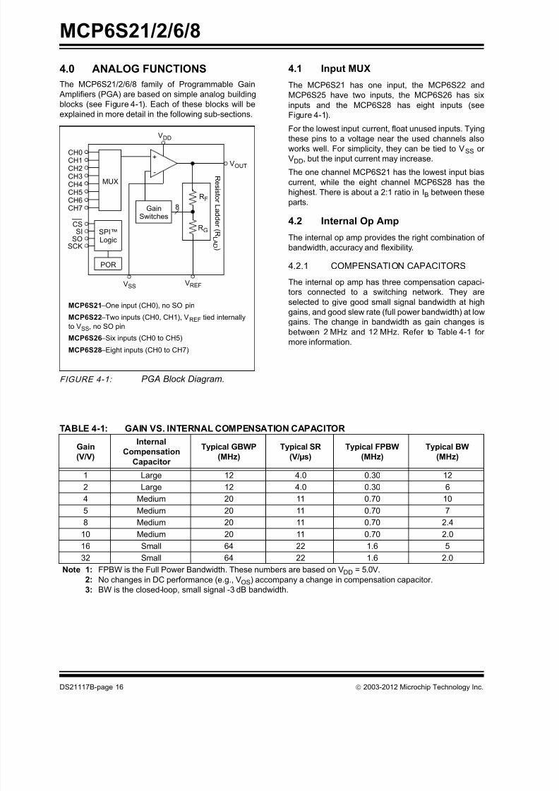
4.0 ANALOG FUNCTIONS
The MCP6S21/2/6/8 family of Programmable Gain
Amplifiers (PGA) are based on simple analog building
blocks (see Figure 4-1). Each of these blocks will be
explained in more detail in the following sub-sections.
FIGURE 4-1: PGA Block Diagram.
4.1 Input MUX
The MCP6S21 has one input, the MCP6S22 and
MCP6S25 have two inputs, the MCP6S26 has six
inputs and the MCP6S28 has eight inputs (see
Figure 4-1).
For the lowest input current, float unused inputs. Tying
these pins to a voltage near the used channels alsoworks well. For simplicity, they can be tied to VSS or
VDD, but the input current may increase.
The one channel MCP6S21 has the lowest input bias
current, while the eight channel MCP6S28 has the
highest. There is about a 2:1 ratio in IB between these
parts.
4.2 Internal Op Amp
The internal op amp provides the right combination of
bandwidth, accuracy and flexibility.
4.2.1 COMPENSATION CAPACITORS
The internal op amp has three compensation capaci-
tors connected to a switching network. They are
selected to give good small signal bandwidth at high
gains, and good slew rate (full power bandwidth) at low
gains. The change in bandwidth as gain changes is
between 2 MHz and 12 MHz. Refer to Table 4-1 for
more information.
TABLE 4-1: GAIN VS. INTERNAL COMPENSATION CAPACITOR
MCP6S21 –One input (CH0), no SO pin
MCP6S22 –Two inputs (CH0, CH1), VREF tied internally
to VSS, no SO pin
MCP6S26 –Six inputs (CH0 to CH5)
MCP6S28 –Eight inputs (CH0 to CH7)
VOUT
VREF
VDD
CSSI
SOSCK
CH1CH0
CH3CH2
CH5CH4
CH7CH6
VSS
8
RF
RG
MUX
SPI™Logic
POR
GainSwitches
+
- R e s i s t or L a d d er ( RL A D )
Gain
(V/V)
Internal
Compensation
Capacitor
Typical GBWP
(MHz)
Typical SR
(V/µs)
Typical FPBW
(MHz)
Typical BW
(MHz)
1 Large 12 4.0 0.30 12
2 Large 12 4.0 0.30 6
4 Medium 20 11 0.70 10
5 Medium 20 11 0.70 7
8 Medium 20 11 0.70 2.4
10 Medium 20 11 0.70 2.0
16 Small 64 22 1.6 5
32 Small 64 22 1.6 2.0
Note 1: FPBW is the Full Power Bandwidth. These numbers are based on VDD = 5.0V.
2: No changes in DC performance (e.g., VOS) accompany a change in compensation capacitor.
3: BW is the closed-loop, small signal -3 dB bandwidth.
8/10/2019 Mcp6s218 Pga
http://slidepdf.com/reader/full/mcp6s218-pga 17/42
2003-2012 Microchip Technology Inc. DS21117B-page 17
MCP6S21/2/6/8
4.2.2 RAIL-TO-RAIL INPUT
The input stage of the internal op amp uses two differ-
ential input stages in parallel; one operates at low VIN
(input voltage), while the other operates at high V IN.
With this topology, the internal inputs can operate to
0.3V past either supply rail. The input offset voltage is
measured at both VIN = VSS - 0.3V and VDD + 0.3V toensure proper operation.
The transition between the two input stages occurs
when VIN VDD - 1.5V. For the best distortion and gain
linearity, avoid this region of operation.
4.2.3 RAIL-TO-RAIL OUTPUT
The Maximum Output Voltage Swing is the maximum
swing possible under a particular output load. Accord-
ing to the specification table, the output can reach
within 60 mV of either supply rail when RL = 10 k and
VREF = VDD/2. See Figure 2-21 for typical performance
under other conditions.
4.2.4 INPUT VOLTAGE AND PHASE
REVERSAL
The amplifier family is designed with CMOS input
devices. It is designed to not exhibit phase inversion
when the input pins exceed the supply voltages.
Figure 2-34 shows an input voltage exceeding both
supplies with no resulting phase inversion.
The maximum voltage that can be applied to the input
pins (CHX) is VSS - 0.3V to VDD + 0.3V. Voltages on the
inputs that exceed this absolute maximum rating can
cause excessive current to flow in or out of the input
pins. Current beyond ±2 mA can cause possible reli-
ability problems. Applications that exceed this rating
must be externally limited with an input resistor, as
shown in Figure 4-2.
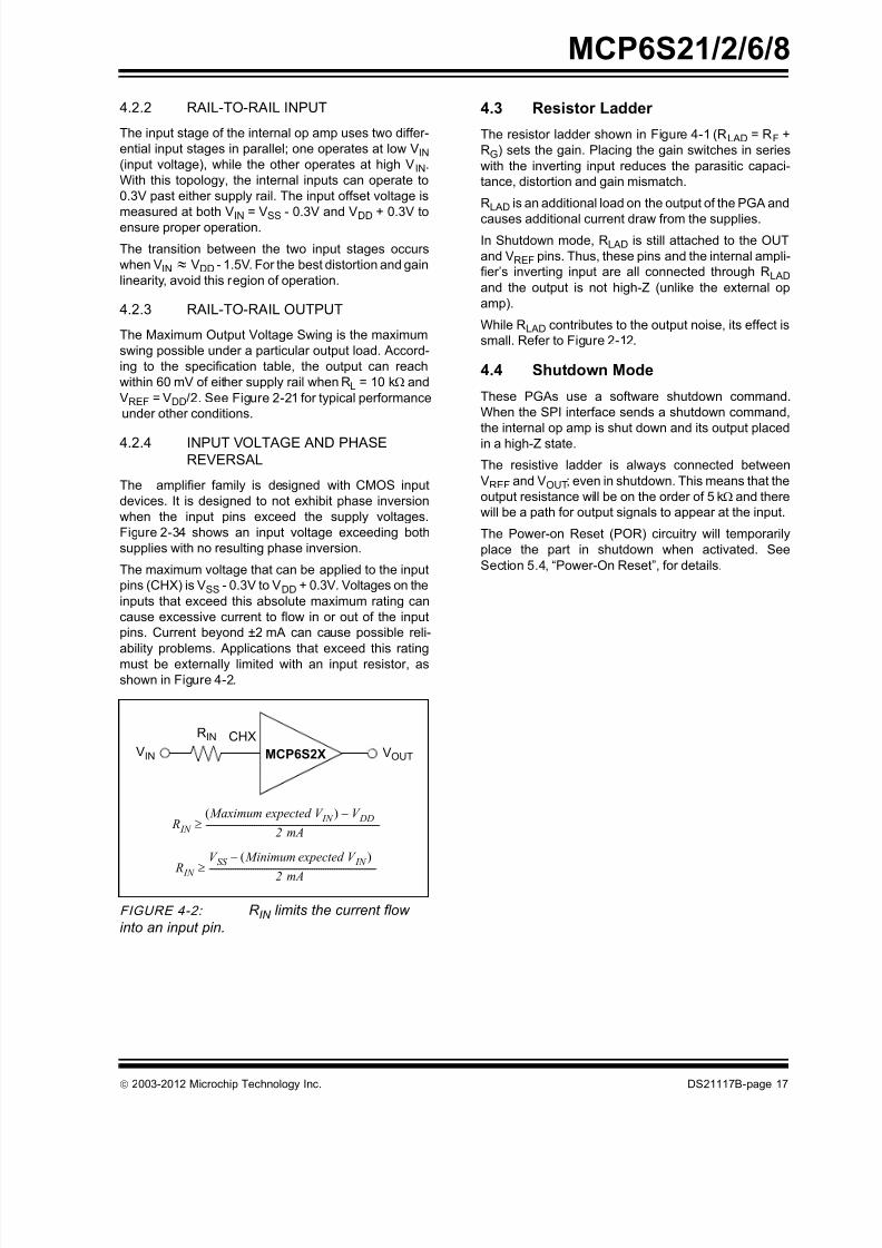
FIGURE 4-2: R IN limits the current flow
into an input pin.
4.3 Resistor Ladder
The resistor ladder shown in Figure 4-1 (RLAD = RF +
RG) sets the gain. Placing the gain switches in series
with the inverting input reduces the parasitic capaci-
tance, distortion and gain mismatch.
RLAD is an additional load on the output of the PGA and
causes additional current draw from the supplies.
In Shutdown mode, RLAD is still attached to the OUT
and VREF pins. Thus, these pins and the internal ampli-
fier’s inverting input are all connected through RLAD
and the output is not high-Z (unlike the external op
amp).
While RLAD contributes to the output noise, its effect is
small. Refer to Figure 2-12.
4.4 Shutdown Mode
These PGAs use a software shutdown command.
When the SPI interface sends a shutdown command,
the internal op amp is shut down and its output placed
in a high-Z state.
The resistive ladder is always connected between
VREF and VOUT; even in shutdown. This means that the
output resistance will be on the order of 5 k and there
will be a path for output signals to appear at the input.
The Power-on Reset (POR) circuitry will temporarily
place the part in shutdown when activated. See
Section 5.4, “Power-On Reset”, for details.
R IN
V SS Minimum expected V IN –
2 mA----------------------------------------------------------------------------
R IN
Maximum expected V IN V DD–
2 mA-------------------------------------------------------------------------------
VIN
RIN
VOUTMCP6S2X
CHX
8/10/2019 Mcp6s218 Pga
http://slidepdf.com/reader/full/mcp6s218-pga 18/42
MCP6S21/2/6/8
DS21117B-page 18 2003-2012 Microchip Technology Inc.
5.0 DIGITAL FUNCTIONS
The MCP6S21/2/6/8 PGAs use a standard SPI com-
patible serial interface to receive instructions from a
controller. This interface is configured to allow daisy
chaining with other SPI devices. There is an internal
POR (Power On Reset) that resets the registers under
low power conditions.
5.1 SPI Timing
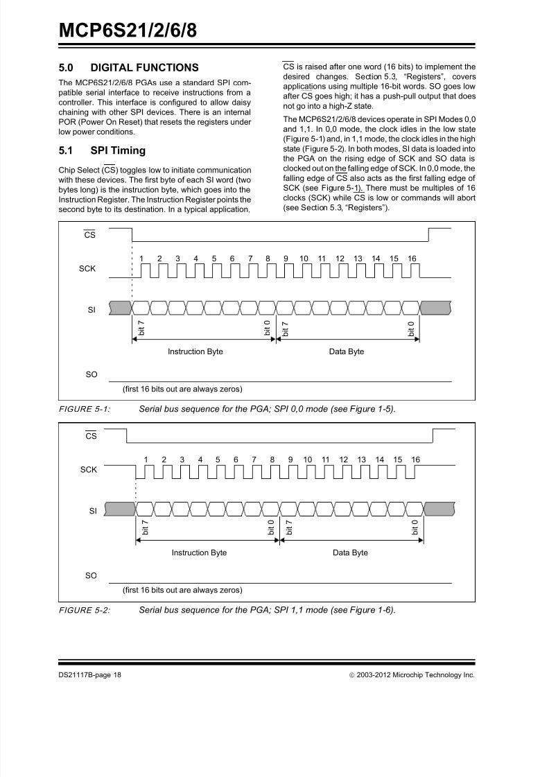
Chip Select (CS) toggles low to initiate communication
with these devices. The first byte of each SI word (two
bytes long) is the instruction byte, which goes into the
Instruction Register. The Instruction Register points the
second byte to its destination. In a typical application,
CS is raised after one word (16 bits) to implement the
desired changes. Section 5.3, “Registers”, covers
applications using multiple 16-bit words. SO goes low
after CS goes high; it has a push-pull output that does
not go into a high-Z state.
The MCP6S21/2/6/8 devices operate in SPI Modes 0,0
and 1,1. In 0,0 mode, the clock idles in the low state
(Figure 5-1) and, in 1,1 mode, the clock idles in the high
state (Figure 5-2). In both modes, SI data is loaded into
the PGA on the rising edge of SCK and SO data is
clocked out on the falling edge of SCK. In 0,0 mode, the
falling edge of CS also acts as the first falling edge of
SCK (see Figure 5-1). There must be multiples of 16
clocks (SCK) while CS is low or commands will abort
(see Section 5.3, “Registers”).
FIGURE 5-1: Serial bus sequence for the PGA; SPI 0,0 mode (see Figure 1-5 ).
FIGURE 5-2: Serial bus sequence for the PGA; SPI 1,1 mode (see Figure 1-6 ).
1 2 3 4 5 6 7 8 9 10 11 12 13 14 15 16
b i t 7
CS
SCK
SI
Instruction Byte Data Byte
b i t 0
b i t 7
b i t 0
SO
(first 16 bits out are always zeros)
1 2 3 4 5 6 7 8 9 10 11 12 13 14 15 16
b i t 7
CS
SCK
SI
Instruction Byte Data Byte
b i t 0
b i t 7
b i t 0
SO
(first 16 bits out are always zeros)
8/10/2019 Mcp6s218 Pga
http://slidepdf.com/reader/full/mcp6s218-pga 19/42
2003-2012 Microchip Technology Inc. DS21117B-page 19
MCP6S21/2/6/8
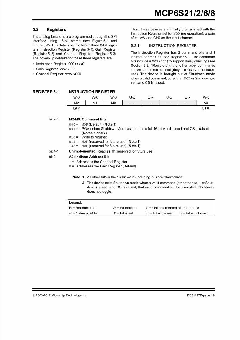
5.2 Registers
The analog functions are programmed through the SPI
interface using 16-bit words (see Figure 5-1 and
Figure 5-2). This data is sent to two of three 8-bit regis-
ters: Instruction Register (Register 5-1), Gain Register
(Register 5-2) and Channel Register (Register 5-3).
The power-up defaults for these three registers are:• Instruction Register: 000x xxx0
• Gain Register: xxxx x000
• Channel Register: xxxx x000
Thus, these devices are initially programmed with the
Instruction Register set for NOP (no operation), a gain
of +1 V/V and CH0 as the input channel.
5.2.1 INSTRUCTION REGISTER
The Instruction Register has 3 command bits and 1
indirect address bit; see Register 5-1. The command
bits include a NOP (000) to support daisy chaining (see
Section 5.3, “Registers”); the other NOP commands
shown should not be used (they are reserved for future
use). The device is brought out of Shutdown mode
when a valid command, other than NOP or Shutdown, is
sent and CS is raised.
REGISTER 5-1: INSTRUCTION REGISTER
W-0 W-0 W-0 U-x U-x U-x U-x W-0
M2 M1 M0 — — — — A0
bit 7 bit 0
bit 7-5 M2-M0: Command Bits000 = NOP (Default) (Note 1)
001 = PGA enters Shutdown Mode as soon as a full 16-bit word is sent and CS is raised.
(Notes 1 and 2)
010 = Write to register.
011 = NOP (reserved for future use) (Note 1)
1XX = NOP (reserved for future use) (Note 1)
bit 4-1 Unimplemented: Read as ‘0’ (reserved for future use)
bit 0 A0: Indirect Address Bit
1 = Addresses the Channel Register
0 = Addresses the Gain Register (Default)
Note 1: All other bits in the 16-bit word (including A0) are “don’t cares”.2: The device exits Shutdown mode when a valid command (other than NOP or Shut-
down) is sent and CS is raised; that valid command will be executed. Shutdown
does not toggle.
Legend:
R = Readable bit W = Writable bit U = Unimplemented bit, read as ‘0’
-n = Value at POR ’1’ = Bit is set ’0’ = Bit is cleared x = Bit is unknown
8/10/2019 Mcp6s218 Pga
http://slidepdf.com/reader/full/mcp6s218-pga 20/42
MCP6S21/2/6/8
DS21117B-page 20 2003-2012 Microchip Technology Inc.
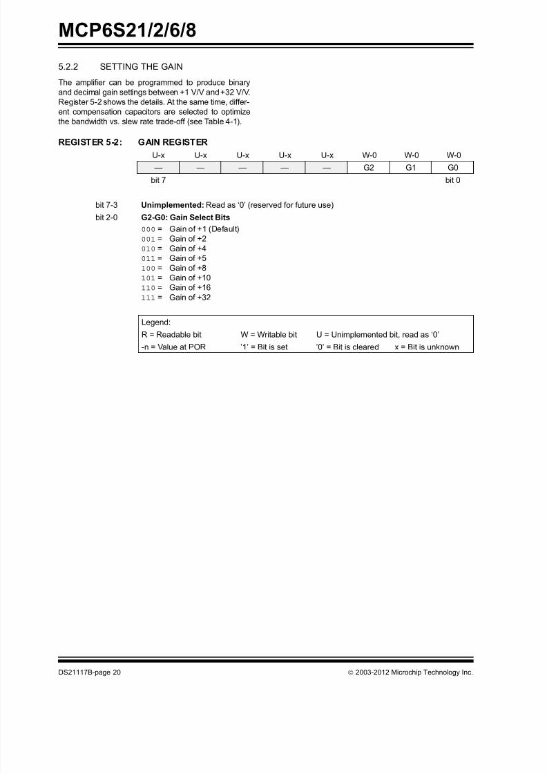
5.2.2 SETTING THE GAIN
The amplifier can be programmed to produce binary
and decimal gain settings between +1 V/V and +32 V/V.
Register 5-2 shows the details. At the same time, differ-
ent compensation capacitors are selected to optimize
the bandwidth vs. slew rate trade-off (see Table 4-1).
REGISTER 5-2: GAIN REGISTER
U-x U-x U-x U-x U-x W-0 W-0 W-0
— — — — — G2 G1 G0
bit 7 bit 0
bit 7-3 Unimplemented: Read as ‘0’ (reserved for future use)
bit 2-0 G2-G0: Gain Select Bits
000 = Gain of +1 (Default)
001 = Gain of +2
010 = Gain of +4
011 = Gain of +5
100 = Gain of +8101 = Gain of +10
110 = Gain of +16
111 = Gain of +32
Legend:
R = Readable bit W = Writable bit U = Unimplemented bit, read as ‘0’
-n = Value at POR ’1’ = Bit is set ’0’ = Bit is cleared x = Bit is unknown
8/10/2019 Mcp6s218 Pga
http://slidepdf.com/reader/full/mcp6s218-pga 21/42
2003-2012 Microchip Technology Inc. DS21117B-page 21
MCP6S21/2/6/8
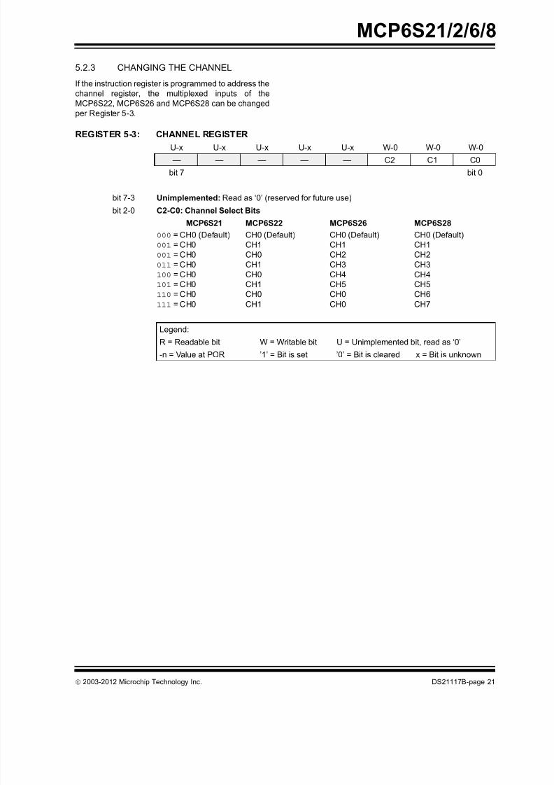
5.2.3 CHANGING THE CHANNEL
If the instruction register is programmed to address the
channel register, the multiplexed inputs of the
MCP6S22, MCP6S26 and MCP6S28 can be changed
per Register 5-3.
REGISTER 5-3: CHANNEL REGISTERU-x U-x U-x U-x U-x W-0 W-0 W-0
— — — — — C2 C1 C0
bit 7 bit 0
bit 7-3 Unimplemented: Read as ‘0’ (reserved for future use)
bit 2-0 C2-C0: Channel Select Bits
MCP6S21
000 = CH0 (Default)
001 = CH0
001 = CH0
011 = CH0
100 = CH0101 = CH0
110 = CH0
111 = CH0
MCP6S22
CH0 (Default)
CH1
CH0
CH1
CH0CH1
CH0
CH1
MCP6S26
CH0 (Default)
CH1
CH2
CH3
CH4CH5
CH0
CH0
MCP6S28
CH0 (Default)
CH1
CH2
CH3
CH4CH5
CH6
CH7
Legend:
R = Readable bit W = Writable bit U = Unimplemented bit, read as ‘0’
-n = Value at POR ’1’ = Bit is set ’0’ = Bit is cleared x = Bit is unknown
8/10/2019 Mcp6s218 Pga
http://slidepdf.com/reader/full/mcp6s218-pga 22/42
MCP6S21/2/6/8
DS21117B-page 22 2003-2012 Microchip Technology Inc.
5.2.4 SHUTDOWN COMMAND
The software Shutdown command allows the user to
put the amplifier into a low power mode (see
Register 5-1). In this shutdown mode, most pins are
high impedance (Section 4.4, “Shutdown Mode”, and
Section 5.1, “SPI Timing”, cover the exceptions at pins
VREF, VOUT and SO).Once the PGA has entered shutdown mode, it will
remain in this mode until either a valid command is sent
to the device (other than NOP or Shutdown), or the
device is powered down and back up again. The
internal registers maintain their values while in
shutdown.
Once brought out of shutdown mode, the part comes
back to its previous state (see Section 5.4 for excep-
tions to this rule). This makes it possible to bring the
device out of shutdown mode using one command;
send a command to select the current channel (or gain)
and the device will exit shutdown with the same state
that existed before shutdown.
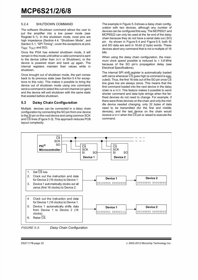
5.3 Daisy Chain Configuration
Multiple devices can be connected in a daisy chain
configuration by connecting the SO pin from one device
to the SI pin on the next device and using common SCK
and CS lines (Figure 5-3). This approach reduces PCB
layout complexity.
The example in Figure 5-3 shows a daisy chain config-
uration with two devices, although any number of
devices can be configured this way. The MCP6S21 and
MCP6S22 can only be used at the far end of the daisy
chain because they do not have a serial data out (SO)
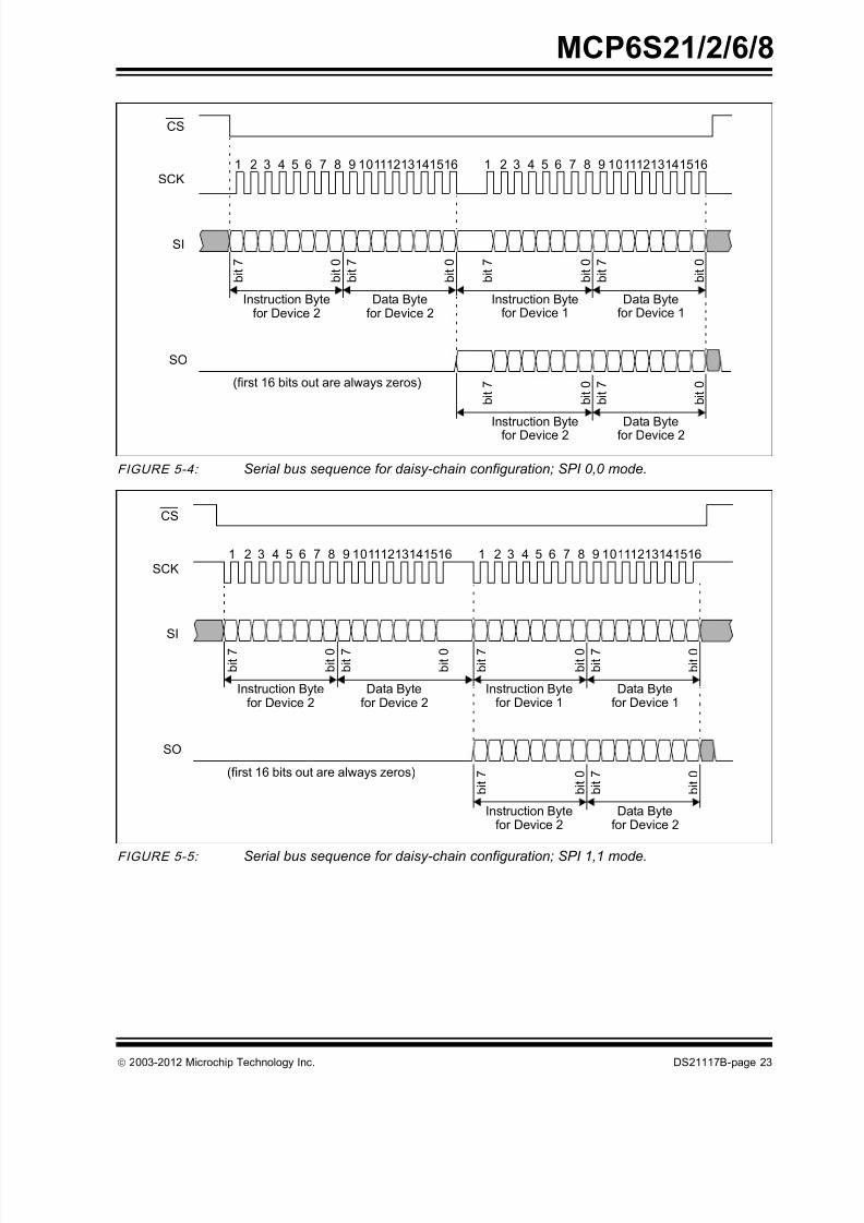
pin. As shown in Figure 5-4 and Figure 5-5, both SI
and SO data are sent in 16-bit (2 byte) words. These
devices abort any command that is not a multiple of 16bits.
When using the daisy chain configuration, the maxi-
mum clock speed possible is reduced to 5.8 MHz
because of the SO pin’s propagation delay (see
Electrical Specifications).
The internal SPI shift register is automatically loaded
with zeros whenever CS goes high (a command is exe-
cuted). Thus, the first 16-bits out of the SO pin once CS
line goes low are always zeros. This means that the
first command loaded into the next device in the daisy
chain is a NOP. This feature makes it possible to send
shorter command and data byte strings when the far-
thest devices do not need to change. For example, if there were three devices on the chain and only the mid-
dle device needed changing, only 32 bytes of data
need to be transmitted (for the first and middle
devices), and the last device on the chain would
receive a NOP when the CS pin is raised to execute the
command.
FIGURE 5-3: Daisy Chain Configuration.
Microcontroller SO
CSSCKSI
CSSCK
SO
Device 1
Device 1
00100000 00000000
SO
CSSCKSI
Device 2
Device 2
00000000 00000000
1. Set CS low.
2. Clock out the instruction and data
for Device 2 (16 clocks) to Device 1.
3. Device 1 automatically clocks out all
zeros (first 16 clocks) to Device 2.
4. Clock out the instruction and data
for Device 1 (16 clocks) to Device 1.
5. Device 1 automatically shifts data
from Device 1 to Device 2 (16
clocks).
6. Raise CS.
Device 1
01000001 00000111
Device 2
00100000 00000000
PIC ®
8/10/2019 Mcp6s218 Pga
http://slidepdf.com/reader/full/mcp6s218-pga 23/42
2003-2012 Microchip Technology Inc. DS21117B-page 23
MCP6S21/2/6/8
FIGURE 5-4: Serial bus sequence for daisy-chain configuration; SPI 0,0 mode.
FIGURE 5-5: Serial bus sequence for daisy-chain configuration; SPI 1,1 mode.
1 2 3 4 5 6 7 8 9 10111213141516
b i t 7
CS
SCK
SI
Instruction Byte Data Byte
b i t 0
b i t 7
b i t 0
SO
(first 16 bits out are always zeros)
1 2 3 4 5 6 7 8 9 10111213141516
b i t 7
Instruction Byte Data Byte
b i t 0
b i t 7
b i t 0
for Device 2 for Device 2 for Device 1 for Device 1
b i t 7
Instruction Byte Data Byte
b i t 0
b i t 7
b i t 0
for Device 2 for Device 2
1 2 3 4 5 6 7 8 9 10111213141516
b i t 7
CS
SCK
SI
Instruction Byte Data Byte
b i t 0
b i t 7
b i t 0
SO
(first 16 bits out are always zeros)
1 2 3 4 5 6 7 8 9 10111213141516
b i t 7
Instruction Byte Data Byte
b i t 0
b i t 7
b i t 0
for Device 2 for Device 2 for Device 1 for Device 1
b i t 7
Instruction Byte Data Byte
b i t 0
b i t 7
b i t 0
for Device 2 for Device 2

8/10/2019 Mcp6s218 Pga
http://slidepdf.com/reader/full/mcp6s218-pga 24/42
MCP6S21/2/6/8
DS21117B-page 24 2003-2012 Microchip Technology Inc.
5.4 Power-On Reset
If the power supply voltage goes below the POR trip
voltage (VDD < VPOR 1.7V), the internal POR circuit
will reset all of the internal registers to their power-up
defaults (this is a protection against low power supply
voltages). The POR circuit also holds the part in shut-
down mode while it is activated. It temporarily overridesthe software shutdown status. The POR releases the
shutdown circuitry once it is released (VDD > VPOR).
A 0.1 µF bypass capacitor mounted as close as possi-
ble to the VDD pin provides additional transient
immunity.
8/10/2019 Mcp6s218 Pga
http://slidepdf.com/reader/full/mcp6s218-pga 25/42
2003-2012 Microchip Technology Inc. DS21117B-page 25
MCP6S21/2/6/8
6.0 APPLICATIONS INFORMATION
6.1 Changing External Reference
Voltage
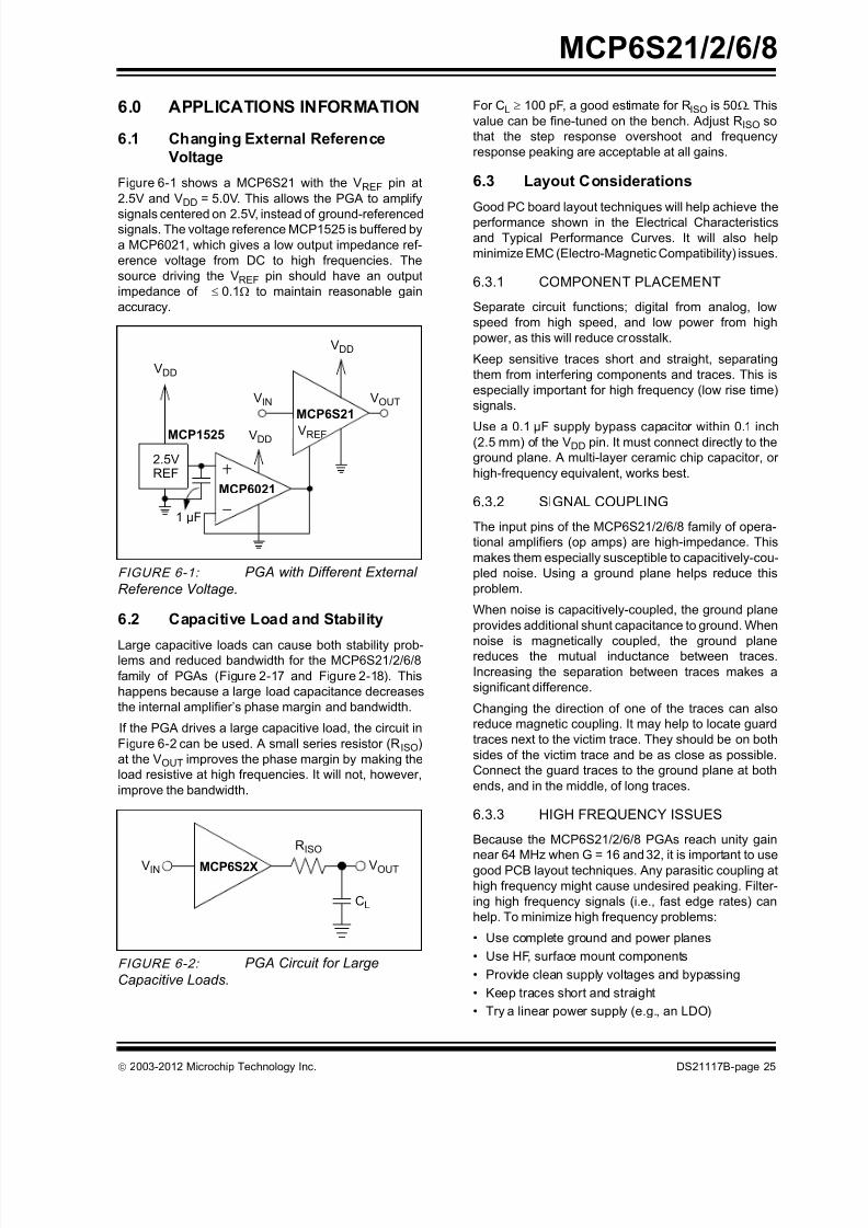
Figure 6-1 shows a MCP6S21 with the VREF pin at
2.5V and VDD = 5.0V. This allows the PGA to amplify
signals centered on 2.5V, instead of ground-referencedsignals. The voltage reference MCP1525 is buffered by
a MCP6021, which gives a low output impedance ref-
erence voltage from DC to high frequencies. The
source driving the VREF pin should have an output
impedance of 0.1 to maintain reasonable gain
accuracy.
FIGURE 6-1: PGA with Different External
Reference Voltage.
6.2 Capacitive Load and Stability
Large capacitive loads can cause both stability prob-lems and reduced bandwidth for the MCP6S21/2/6/8
family of PGAs (Figure 2-17 and Figure 2-18). This
happens because a large load capacitance decreases
the internal amplifier’s phase margin and bandwidth.
If the PGA drives a large capacitive load, the circuit in
Figure 6-2 can be used. A small series resistor (R ISO)
at the VOUT improves the phase margin by making the
load resistive at high frequencies. It will not, however,
improve the bandwidth.
FIGURE 6-2: PGA Circuit for Large
Capacitive Loads.
For CL 100 pF, a good estimate for RISO is 50. This
value can be fine-tuned on the bench. Adjust RISO so
that the step response overshoot and frequency
response peaking are acceptable at all gains.
6.3 Layout Considerations
Good PC board layout techniques will help achieve the
performance shown in the Electrical Characteristics
and Typical Performance Curves. It will also help
minimize EMC (Electro-Magnetic Compatibility) issues.
6.3.1 COMPONENT PLACEMENT
Separate circuit functions; digital from analog, low
speed from high speed, and low power from high
power, as this will reduce crosstalk.
Keep sensitive traces short and straight, separating
them from interfering components and traces. This is
especially important for high frequency (low rise time)
signals.
Use a 0.1 µF supply bypass capacitor within 0.1 inch(2.5 mm) of the VDD pin. It must connect directly to the
ground plane. A multi-layer ceramic chip capacitor, or
high-frequency equivalent, works best.
6.3.2 SIGNAL COUPLING
The input pins of the MCP6S21/2/6/8 family of opera-
tional amplifiers (op amps) are high-impedance. This
makes them especially susceptible to capacitively-cou-
pled noise. Using a ground plane helps reduce this
problem.
When noise is capacitively-coupled, the ground plane
provides additional shunt capacitance to ground. When
noise is magnetically coupled, the ground planereduces the mutual inductance between traces.
Increasing the separation between traces makes a
significant difference.
Changing the direction of one of the traces can also
reduce magnetic coupling. It may help to locate guard
traces next to the victim trace. They should be on both
sides of the victim trace and be as close as possible.
Connect the guard traces to the ground plane at both
ends, and in the middle, of long traces.
6.3.3 HIGH FREQUENCY ISSUES
Because the MCP6S21/2/6/8 PGAs reach unity gain
near 64 MHz when G = 16 and 32, it is important to usegood PCB layout techniques. Any parasitic coupling at
high frequency might cause undesired peaking. Filter-
ing high frequency signals (i.e., fast edge rates) can
help. To minimize high frequency problems:
• Use complete ground and power planes
• Use HF, surface mount components
• Provide clean supply voltages and bypassing
• Keep traces short and straight
• Try a linear power supply (e.g., an LDO)
VDD
VREF
MCP6S21
MCP1525
MCP6021
2.5VREF
VDD
VDD
VIN VOUT
1 µF
VIN MCP6S2X
RISO
VOUT
CL
8/10/2019 Mcp6s218 Pga
http://slidepdf.com/reader/full/mcp6s218-pga 26/42
MCP6S21/2/6/8
DS21117B-page 26 2003-2012 Microchip Technology Inc.
6.4 Typical Applications
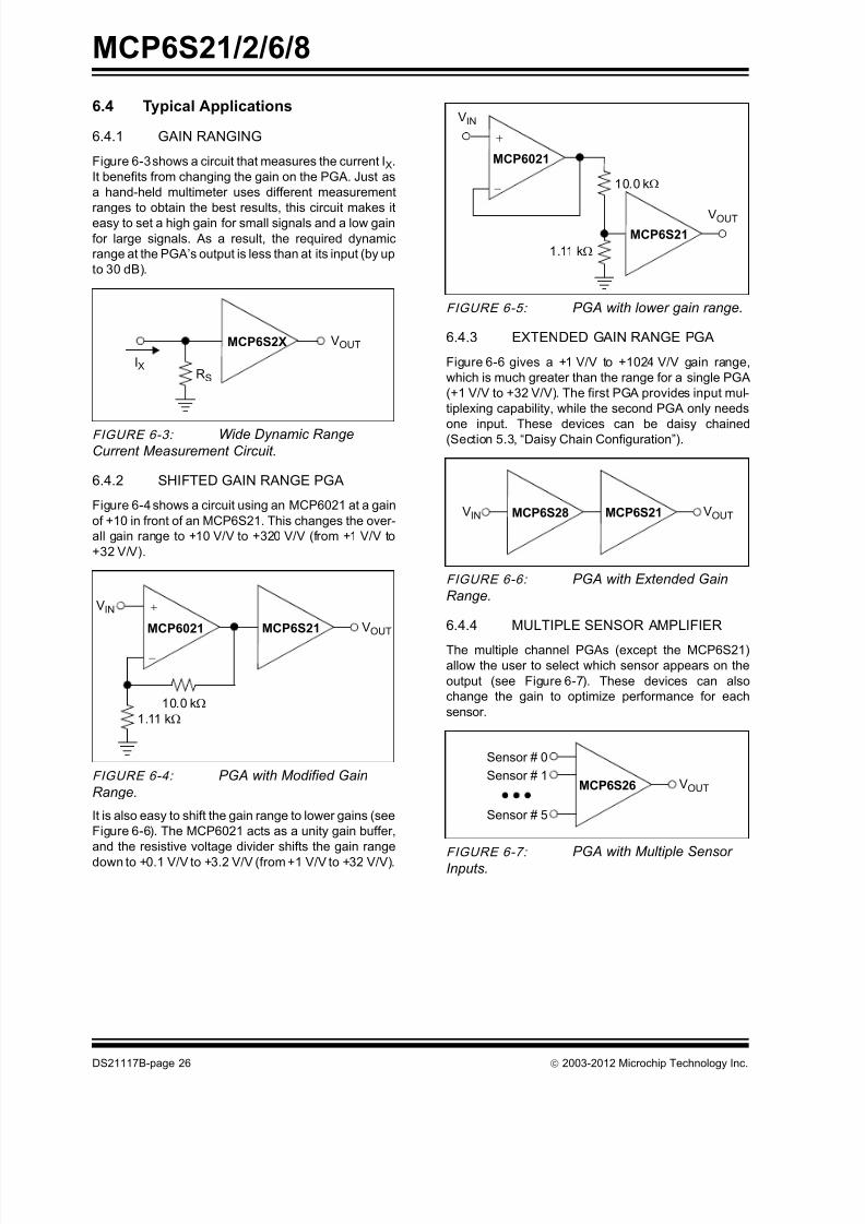
6.4.1 GAIN RANGING
Figure 6-3 shows a circuit that measures the current IX.
It benefits from changing the gain on the PGA. Just as
a hand-held multimeter uses different measurement
ranges to obtain the best results, this circuit makes iteasy to set a high gain for small signals and a low gain
for large signals. As a result, the required dynamic
range at the PGA’s output is less than at its input (by up
to 30 dB).
FIGURE 6-3: Wide Dynamic Range
Current Measurement Circuit.
6.4.2 SHIFTED GAIN RANGE PGA
Figure 6-4 shows a circuit using an MCP6021 at a gain
of +10 in front of an MCP6S21. This changes the over-
all gain range to +10 V/V to +320 V/V (from +1 V/V to
+32 V/V).
FIGURE 6-4: PGA with Modified Gain
Range.
It is also easy to shift the gain range to lower gains (see
Figure 6-6). The MCP6021 acts as a unity gain buffer,
and the resistive voltage divider shifts the gain range
down to +0.1 V/V to +3.2 V/V (from +1 V/V to +32 V/V).
FIGURE 6-5: PGA with lower gain range.
6.4.3 EXTENDED GAIN RANGE PGA
Figure 6-6 gives a +1 V/V to +1024 V/V gain range,
which is much greater than the range for a single PGA
(+1 V/V to +32 V/V). The first PGA provides input mul-
tiplexing capability, while the second PGA only needs
one input. These devices can be daisy chained(Section 5.3, “Daisy Chain Configuration”).
FIGURE 6-6: PGA with Extended Gain
Range.
6.4.4 MULTIPLE SENSOR AMPLIFIER
The multiple channel PGAs (except the MCP6S21)
allow the user to select which sensor appears on the
output (see Figure 6-7). These devices can also
change the gain to optimize performance for each
sensor.
FIGURE 6-7:
PGA with Multiple SensorInputs.
MCP6S2X VOUT
IXRS
VIN
MCP6021 MCP6S21 VOUT
10.0 k1.11 k
VIN
MCP6021
MCP6S21
VOUT
10.0 k
1.11 k
VIN VOUTMCP6S28 MCP6S21
Sensor # 0
Sensor # 1
Sensor # 5
MCP6S26 VOUT
8/10/2019 Mcp6s218 Pga
http://slidepdf.com/reader/full/mcp6s218-pga 27/42
2003-2012 Microchip Technology Inc. DS21117B-page 27
MCP6S21/2/6/8
6.4.5 EXPANDED INPUT PGA
Figure 6-8 shows cascaded MCP6S28s that provide
up to 15 input channels. Obviously, Sensors #7-14
have a high total gain range available, as explained in
Section 6.4.3, “Extended Gain Range”. These devices
can be daisy chained (Section 5.3, “Daisy Chain
Configuration”).
FIGURE 6-8: PGA with Expanded Inputs.
6.4.6 PIC MCU WITH EXPANDED INPUT
CAPABILITY
Figure 6-9 shows an MCP6S28 driving an analog input
to a PIC microcontroller. This greatly expands the input
capacity of the microcontroller, while adding the ability
to select the appropriate gain for each source.
FIGURE 6-9: Expanded Input for a PIC ®
Microcontroller.
6.4.7 ADC DRIVER
The family of PGA’s is well suited for driving Analog-to-
Digital Converters (ADC). The binary gains (1, 2, 4, 8,
16 and 32) effectively add five more bits to the input
range (see Figure 6-10). This works well for applica-
tions needing relative accuracy more than absolute
accuracy (e.g., power monitoring).
FIGURE 6-10: PGA as an ADC Driver.
At low gains, the ADC’s Signal-to-Noise Ratio (SNR)
will dominate since the PGAs input noise voltage den-
sity is so low (10 nV/Hz @ 10 kHz, typ.). At high gains,
the PGA’s noise will dominate the SNR, but its low
noise supports most applications. Again, these PGAsadd the flexibility of selecting the best gain for an
application.
The low pass filter in the block diagram reduces the
integrated noise at the MCP6S28’s output and serves
as an anti-aliasing filter. This filter may be designed
using Microchip’s FilterLab® software, available at
www.microchip.com.
Sensors
SensorsMCP6S28
MCP6S28 VOUT
# 0-6
# 7-14
VIN MCP6S28PIC®
Microcontroller
SPI™
VIN OUTMCP6S28
LowpassFilter
12MCP3201
8/10/2019 Mcp6s218 Pga
http://slidepdf.com/reader/full/mcp6s218-pga 28/42
MCP6S21/2/6/8
DS21117B-page 28 2003-2012 Microchip Technology Inc.
7.0 PACKAGING INFORMATION
7.1 Package Marking Information
XXXXXXXXXXXXXNNN
YYWW
8-Lead PDIP (300 mil) (MCP6S21, MCP6S22) Example:
8-Lead SOIC (150 mil) (MCP6S21, MCP6S22) Example:
XXXXXXXX
XXXXYYWW
NNN
MCP6S21I/P256
0345
MCP6S21
I/SN0345
256
8-Lead MSOP (MCP6S21, MCP6S22) Example:
XXXXX
YWWNNN
MCP6S21I
345256
Legend: XX...X Customer specific information*
YY Year code (last 2 digits of calendar year)
WW Week code (week of January 1 is week ‘01’)
NNN Alphanumeric traceability code
Note: In the event the full Microchip part number cannot be marked on one line, it will
be carried over to the next line thus limiting the number of available characters
for customer specific information.
* Standard marking consists of Microchip part number, year code, week code, traceability code (facility
code, mask rev#, and assembly code). For marking beyond this, certain price adders apply. Please check
with your Microchip Sales Office.
8/10/2019 Mcp6s218 Pga
http://slidepdf.com/reader/full/mcp6s218-pga 29/42
2003-2012 Microchip Technology Inc. DS21117B-page 29
MCP6S21/2/6/8
Package Marking Information (Con’t)
14-Lead PDIP (300 mil) (MCP6S26) Example:
14-Lead SOIC (150 mil) (MCP6S26) Example:
XXXXXXXXXXXXXX
XXXXXXXXXXXXXX
YYWWNNN
XXXXXXXXXXX
YYWWNNN
MCP6S26-I/P
XXXXXXXXXXXXXX
0345256
XXXXXXXXXXX
MCP6S26ISL
0345256
XXXXXXXXXXXXXXXXXXXXXXXXX
XXXXXXXX
NNN
YYWW
14-Lead TSSOP (4.4mm) (MCP6S26) Example:
MCP6S26IST
256
0345
8/10/2019 Mcp6s218 Pga
http://slidepdf.com/reader/full/mcp6s218-pga 30/42
8/10/2019 Mcp6s218 Pga
http://slidepdf.com/reader/full/mcp6s218-pga 31/42
2003-2012 Microchip Technology Inc. DS21117B-page 31
MCP6S21/2/6/8
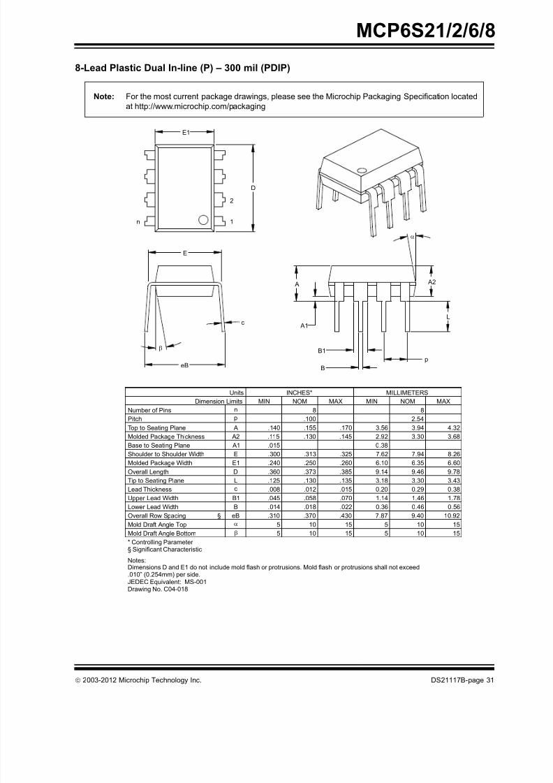
8-Lead Plastic Dual In-line (P) – 300 mil (PDIP)
B1
B
A1
A
L
A2
p
E
eB
c
E1
n
D
1
2
Units INCHES* MILLIMETERS
Dimension Limits MIN NOM MAX MIN NOM MAX
Number of Pins n 8 8Pitch p .100 2.54
Top to Seating Plane A .140 .155 .170 3.56 3.94 4.32
Molded Package Thickness A2 .115 .130 .145 2.92 3.30 3.68
Base to Seating Plane A1 .015 0.38
Shoulder to Shoulder Width E .300 .313 .325 7.62 7.94 8.26
Molded Package Width E1 .240 .250 .260 6.10 6.35 6.60
Overall Length D .360 .373 .385 9.14 9.46 9.78
Tip to Seating Plane L .125 .130 .135 3.18 3.30 3.43
Lead Thickness c .008 .012 .015 0.20 0.29 0.38
Upper Lead Width B1 .045 .058 .070 1.14 1.46 1.78
Lower Lead Width B .014 .018 .022 0.36 0.46 0.56
Overall Row Spacing § eB .310 .370 .430 7.87 9.40 10.92
Mold Draft Angle Top 5 10 15 5 10 15
Mold Draft Angle Bottom 5 10 15 5 10 15
* Controlling Parameter
Notes:Dimensions D and E1 do not include mold flash or protrusions. Mold flash or protrusions shall not exceed
JEDEC Equivalent: MS-001Drawing No. C04-018
.010” (0.254mm) per side.
§ Significant Characteristic
Note: For the most current package drawings, please see the Microchip Packaging Specification located
at http://www.microchip.com/packaging
8/10/2019 Mcp6s218 Pga
http://slidepdf.com/reader/full/mcp6s218-pga 32/42
MCP6S21/2/6/8
DS21117B-page 32 2003-2012 Microchip Technology Inc.
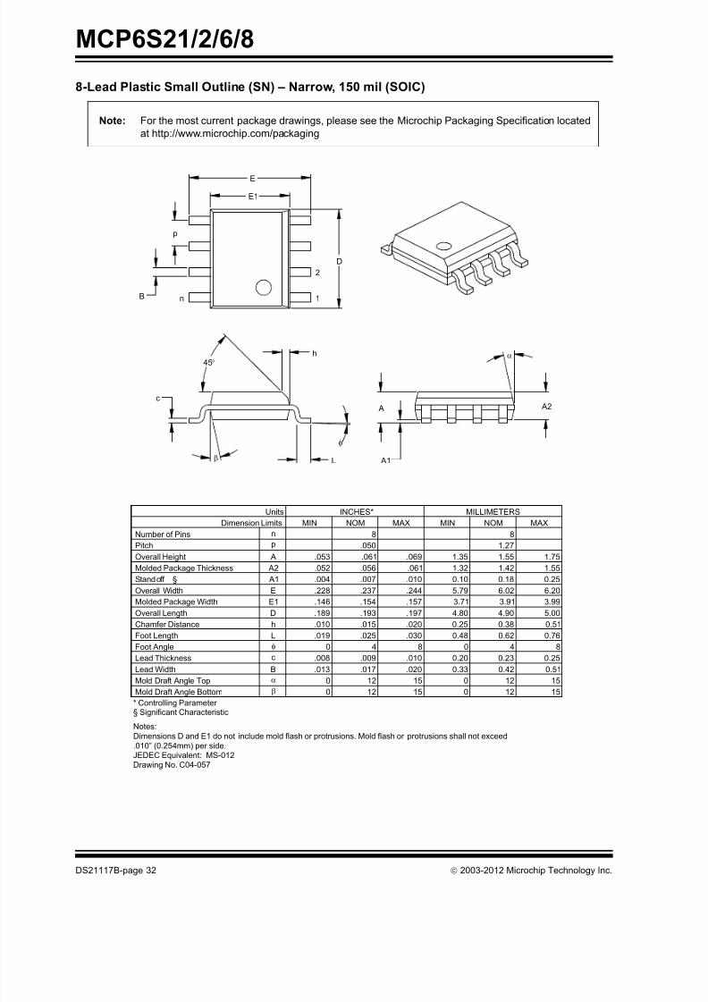
8-Lead Plastic Small Outline (SN) – Narrow, 150 mil (SOIC)
Foot Angle 0 4 8 0 4 8
1512015120Mold Draft Angle Bottom
1512015120Mold Draft Angle Top
0.510.420.33.020.017.013BLead Width
0.250.230.20.010.009.008cLead Thickness
0.760.620.48.030.025.019LFoot Length
0.510.380.25.020.015.010hChamfer Distance
5.004.904.80.197.193.189DOverall Length
3.993.913.71.157.154.146E1Molded Package Width
6.206.025.79.244.237.228EOverall Width
0.250.180.10.010.007.004 A1Standoff §
1.551.421.32.061.056.052 A2Molded Package Thickness
1.751.551.35.069.061.053 AOverall Height
1.27.050pPitch
88nNumber of PinsMAXNOMMINMAXNOMMINDimension Limits
MILLIMETERSINCHES*Units
2
1
D
n
p
B
E
E1
h
L
c
45
A2
A
A1
* Controlling Parameter
Notes:
Dimensions D and E1 do not include mold flash or protrusions. Mold flash or protrusions shall not exceed
.010” (0.254mm) per side.JEDEC Equivalent: MS-012Drawing No. C04-057
§ Significant Characteristic
Note: For the most current package drawings, please see the Microchip Packaging Specification located
at http://www.microchip.com/packaging
8/10/2019 Mcp6s218 Pga
http://slidepdf.com/reader/full/mcp6s218-pga 33/42
2003-2012 Microchip Technology Inc. DS21117B-page 33
MCP6S21/2/6/8
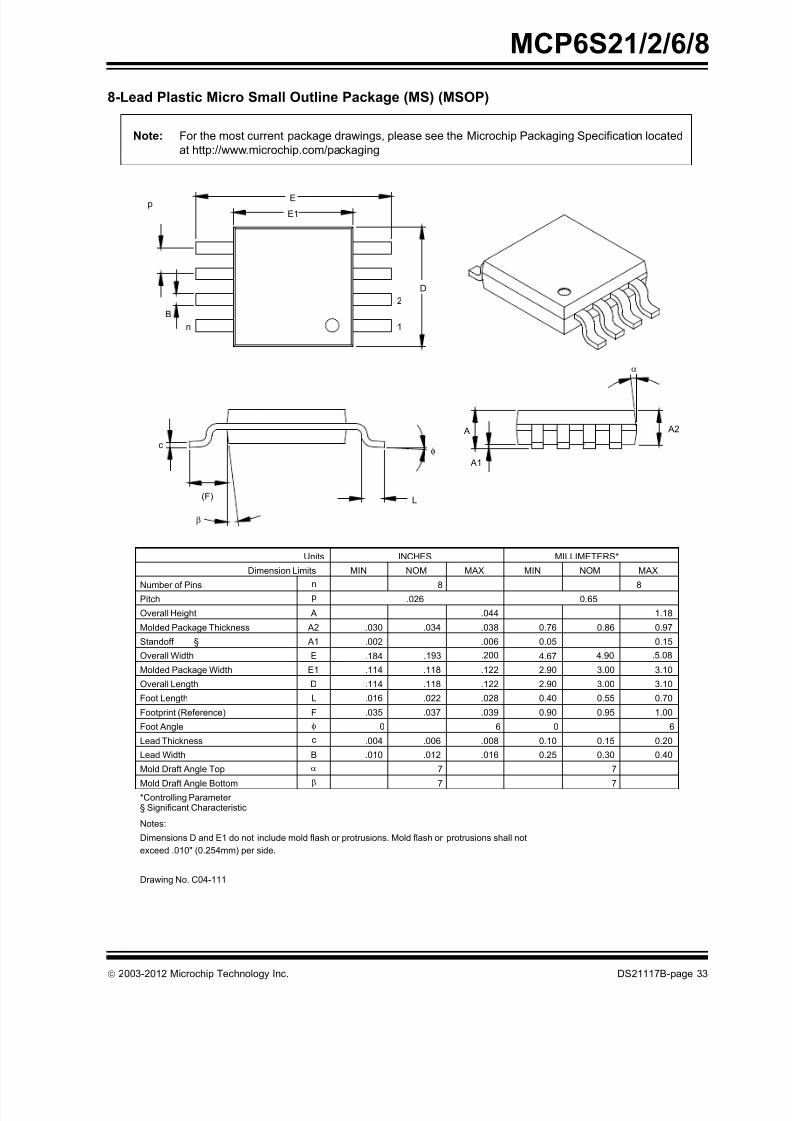
8-Lead Plastic Micro Small Outline Package (MS) (MSOP)
p
A
A1
A2
D
L
c
Dimensions D and E1 do not include mold flash or protrusions. Mold flash or protrusions shall not
.037.035FFootprint (Reference)
exceed .010" (0.254mm) per side.
Notes:
Drawing No. C04-111
*Controlling Parameter
Mold Draft Angle Top
Mold Draft Angle Bottom
Foot Angle
Lead Width
Lead Thickness
c
B
7
7
.004
.010
0
.006
.012
(F)
Dimension Limits
Overall Height
Molded Package Thickness
Molded Package Width
Overall Length
Foot Length
Standoff §
Overall Width
Number of PinsPitch
A
L
E1
D
A1
E
A2
.016
.114
.114
.022
.118
.118
.002
.030
.193
.034
MIN
p
n
Units
.026
NOM
8
INCHES
1.000.950.90.039
0.15
0.30
.008
.016
6
0.10
0.25
0
7
7
0.20
0.40
6
MILLIMETERS*
0.65
0.86
3.00
3.00
0.55
4.90
.044
.122
.028
.122
.038
.006
0.40
2.90
2.90
0.05
0.76
MINMAX NOM
1.18
0.70
3.10
3.10
0.15
0.97
MAX
8
E1
E
B
n 1
2
§ Significant Characteristic
.184 .200 4.67 .5.08
Note: For the most current package drawings, please see the Microchip Packaging Specification located
at http://www.microchip.com/packaging
8/10/2019 Mcp6s218 Pga
http://slidepdf.com/reader/full/mcp6s218-pga 34/42
MCP6S21/2/6/8
DS21117B-page 34 2003-2012 Microchip Technology Inc.
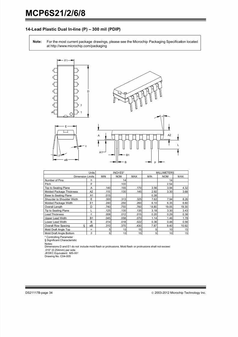
14-Lead Plastic Dual In-line (P) – 300 mil (PDIP)
E1
n
D
1
2
eB
E
c
A
A1
B
B1
L
A2
p
Units INCHES* MILLIMETERS
Dimension Limits MIN NOM MAX MIN NOM MAXNumber of Pins n 14 14
Pitch p .100 2.54
Top to Seating Plane A .140 .155 .170 3.56 3.94 4.32
Molded Package Thickness A2 .115 .130 .145 2.92 3.30 3.68
Base to Seating Plane A1 .015 0.38
Shoulder to Shoulder Width E .300 .313 .325 7.62 7.94 8.26
Molded Package Width E1 .240 .250 .260 6.10 6.35 6.60
Overall Length D .740 .750 .760 18.80 19.05 19.30
Tip to Seating Plane L .125 .130 .135 3.18 3.30 3.43
Lead Thickness c .008 .012 .015 0.20 0.29 0.38
Upper Lead Width B1 .045 .058 .070 1.14 1.46 1.78
Lower Lead Width B .014 .018 .022 0.36 0.46 0.56
Overall Row Spacing § eB .310 .370 .430 7.87 9.40 10.92
Mold Draft Angle Top 5 10 15 5 10 15
5 10 15 5 10 15Mold Draft Angle Bottom
* Controlling Parameter
Notes:Dimensions D and E1 do not include mold flash or protrusions. Mold flash or protrusions shall not exceed
.010” (0.254mm) per side.JEDEC Equivalent: MS-001Drawing No. C04-005
§ Significant Characteristic
Note: For the most current package drawings, please see the Microchip Packaging Specification located
at http://www.microchip.com/packaging
8/10/2019 Mcp6s218 Pga
http://slidepdf.com/reader/full/mcp6s218-pga 35/42
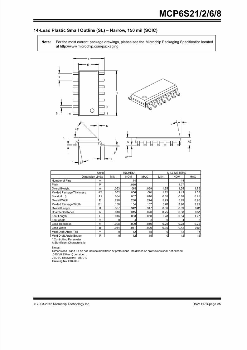
2003-2012 Microchip Technology Inc. DS21117B-page 35
MCP6S21/2/6/8
14-Lead Plastic Small Outline (SL) – Narrow, 150 mil (SOIC)
Foot Angle 0 4 8 0 4 8
1512015120Mold Draft Angle Bottom
1512015120Mold Draft Angle Top
0.510.420.36.020.017.014BLead Width
0.250.230.20.010.009.008cLead Thickness
1.270.840.41.050.033.016LFoot Length
0.510.380.25.020.015.010hChamfer Distance
8.818.698.56.347.342.337DOverall Length
3.993.903.81.157.154.150E1Molded Package Width
6.205.995.79.244.236.228EOverall Width
0.250.180.10.010.007.004 A1Standoff §
1.551.421.32.061.056.052 A2Molded Package Thickness
1.751.551.35.069.061.053 AOverall Height
1.27.050pPitch
1414nNumber of Pins
MAXNOMMINMAXNOMMINDimension Limits
MILLIMETERSINCHES*Units
2
1
D
p
nB
E
E1
h
L
c
45
A2 A
A1
* Controlling Parameter
Notes:
Dimensions D and E1 do not include mold flash or protrusions. Mold flash or protrusions shall not exceed
.010” (0.254mm) per side.
JEDEC Equivalent: MS-012
Drawing No. C04-065
§ Significant Characteristic
Note: For the most current package drawings, please see the Microchip Packaging Specification located
at http://www.microchip.com/packaging
8/10/2019 Mcp6s218 Pga
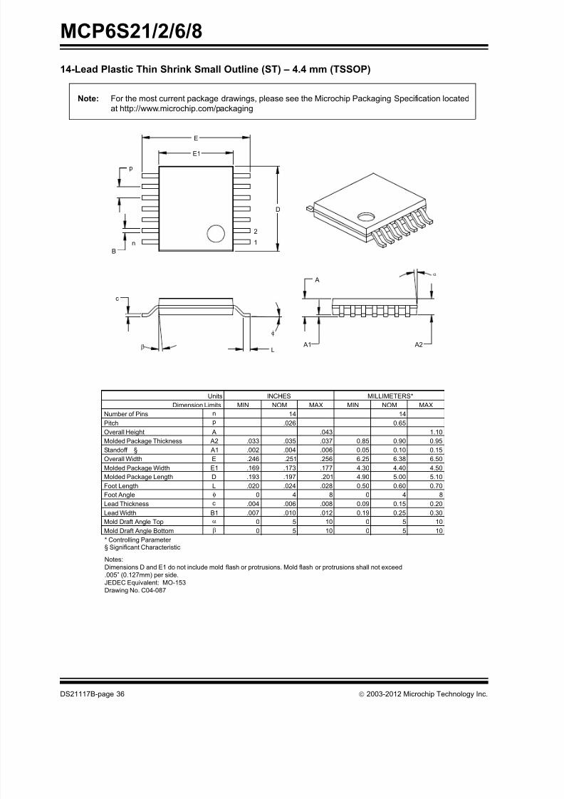
http://slidepdf.com/reader/full/mcp6s218-pga 36/42
8/10/2019 Mcp6s218 Pga
http://slidepdf.com/reader/full/mcp6s218-pga 37/42
2003-2012 Microchip Technology Inc. DS21117B-page 37
MCP6S21/2/6/8
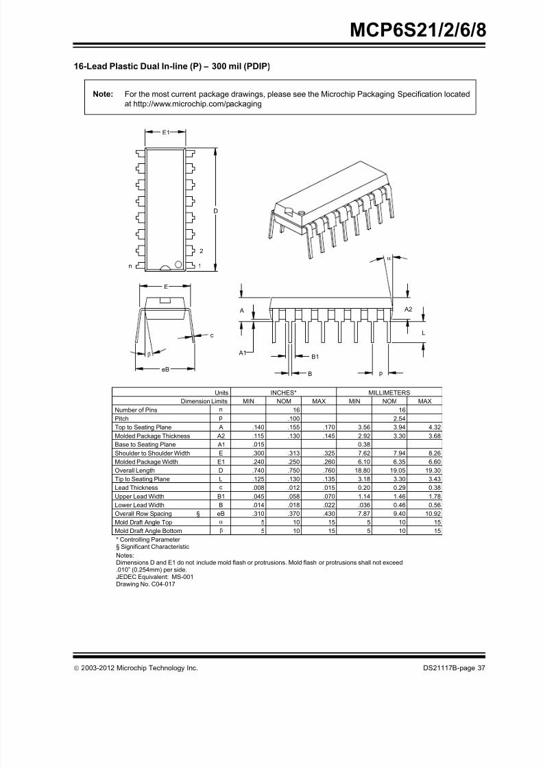
16-Lead Plastic Dual In-line (P) – 300 mil (PDIP)
1510515105Mold Draft Angle Bottom
1510515105Mold Draft Angle Top
10.929.407.87.430.370.310eBOverall Row Spacing §
0.560.46.036.022.018.014BLower Lead Width
1.781.461.14.070.058.045B1Upper Lead Width
0.380.290.20.015.012.008cLead Thickness
3.433.303.18.135.130.125LTip to Seating Plane
19.3019.0518.80.760.750.740DOverall Length
6.606.356.10.260.250.240E1Molded Package Width
8.267.947.62.325.313.300EShoulder to Shoulder Width
0.38.015 A1Base to Seating Plane
3.683.302.92.145.130.115 A2Molded Package Thickness
4.323.943.56.170.155.140 ATop to Seating Plane
2.54.100pPitch
1616nNumber of PinsMAXNOMMINMAXNOMMINDimension Limits
MILLIMETERSINCHES*Units
2
1
D
n
E1
c
eB
E
p
L
A2
B
B1
A
A1
* Controlling Parameter
Notes:Dimensions D and E1 do not include mold flash or protrusions. Mold flash or protrusions shall not exceed.010” (0.254mm) per side.JEDEC Equivalent: MS-001Drawing No. C04-017
§ Significant Characteristic
Note: For the most current package drawings, please see the Microchip Packaging Specification located
at http://www.microchip.com/packaging
8/10/2019 Mcp6s218 Pga
http://slidepdf.com/reader/full/mcp6s218-pga 38/42
MCP6S21/2/6/8
DS21117B-page 38 2003-2012 Microchip Technology Inc.
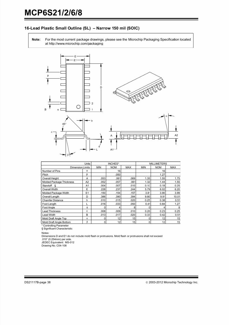
16-Lead Plastic Small Outline (SL) – Narrow 150 mil (SOIC)
Foot Angle 0 4 8 0 4 8
1512015120Mold Draft Angle Bottom
1512015120Mold Draft Angle Top
0.510.420.33.020.017.013BLead Width
0.250.230.20.010.009.008cLead Thickness
1.270.840.41.050.033.016LFoot Length
0.510.380.25.020.015.010hChamfer Distance
10.019.919.80.394.390.386DOverall Length
3.993.903.81.157.154.150E1Molded Package Width
6.206.025.79.244.237.228EOverall Width
0.250.180.10.010.007.004 A1Standoff §
1.551.441.32.061.057.052 A2Molded Package Thickness
1.751.551.35.069.061.053 AOverall Height
1.27.050pPitch1616nNumber of Pins
MAXNOMMINMAXNOMMINDimension Limits
MILLIMETERSINCHES*Units
A2
E1
1
2
L
h
nB
45
E
p
D
c
A1
A
* Controlling Parameter
Notes:Dimensions D and E1 do not include mold flash or protrusions. Mold flash or protrusions shall not exceed
.010” (0.254mm) per side.
JEDEC Equivalent: MS-012
Drawing No. C04-108
§ Significant Characteristic
Note: For the most current package drawings, please see the Microchip Packaging Specification located
at http://www.microchip.com/packaging
8/10/2019 Mcp6s218 Pga
http://slidepdf.com/reader/full/mcp6s218-pga 39/42
2003-2012 Microchip Technology Inc. DS21117B-page 39
MCP6S21/2/6/8
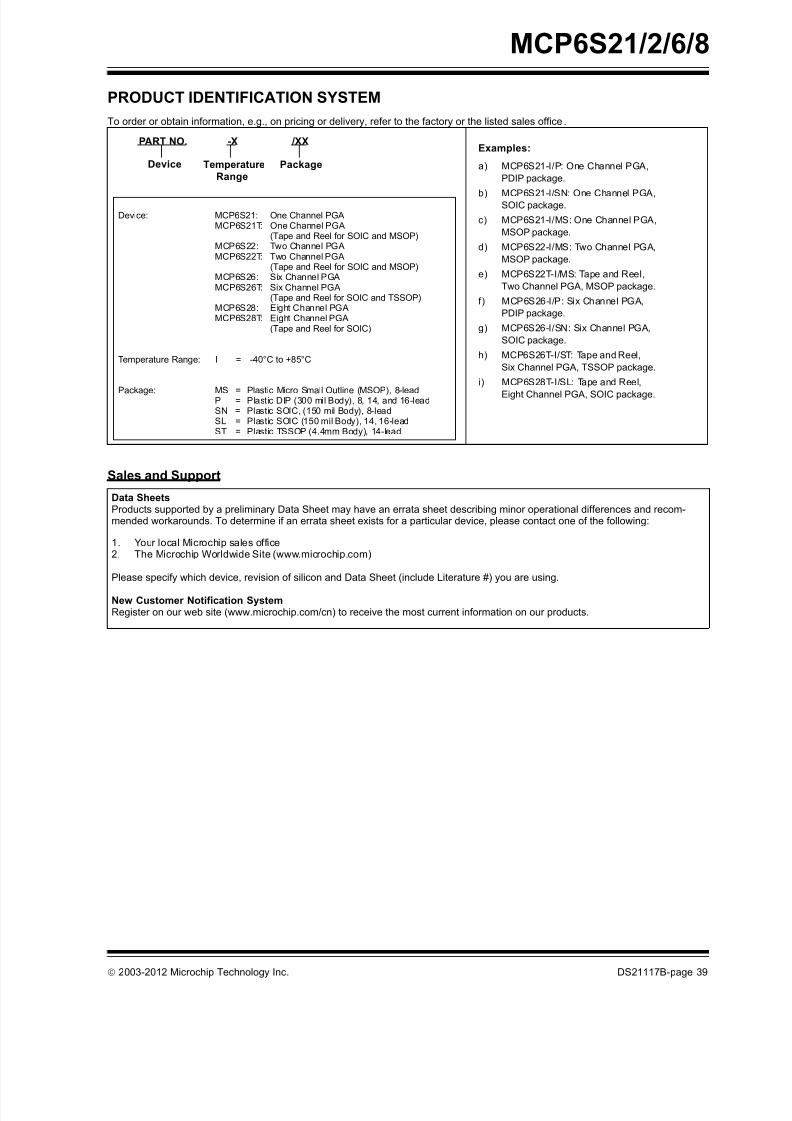
PRODUCT IDENTIFICATION SYSTEM
To order or obtain information, e.g., on pricing or delivery, refer to the factory or the listed sales office.
Sales and Support
Data SheetsProducts supported by a preliminary Data Sheet may have an errata sheet describing minor operational differences and recom-mended workarounds. To determine if an errata sheet exists for a particular device, please contact one of the following:
1. Your local Microchip sales office2. The Microchip Worldwide Site (www.microchip.com)
Please specify which device, revision of silicon and Data Sheet (include Literature #) you are using.
New Customer Notification SystemRegister on our web site (www.microchip.com/cn) to receive the most current information on our products.
PART NO. -X /XX
PackageTemperature
Range
Device
Device: MCP6S21: One Channel PGAMCP6S21T: One Channel PGA
(Tape and Reel for SOIC and MSOP)MCP6S22: Two Channel PGAMCP6S22T: Two Channel PGA
(Tape and Reel for SOIC and MSOP)MCP6S26: Six Channel PGAMCP6S26T: Six Channel PGA
(Tape and Reel for SOIC and TSSOP)MCP6S28: Eight Channel PGAMCP6S28T: Eight Channel PGA
(Tape and Reel for SOIC)
Temperature Range: I = -40°C to +85°C
Package: MS = Plastic Micro Small Outline (MSOP), 8-leadP = Plastic DIP (300 mil Body), 8, 14, and 16-leadSN = Plastic SOIC, (150 mil Body), 8-leadSL = Plastic SOIC (150 mil Body), 14, 16-leadST = Plastic TSSOP (4.4mm Body), 14-lead
Examples:
a) MCP6S21-I/P: One Channel PGA,
PDIP package.
b) MCP6S21-I/SN: One Channel PGA,SOIC package.
c) MCP6S21-I/MS: One Channel PGA,
MSOP package.
d) MCP6S22-I/MS: Two Channel PGA,
MSOP package.
e) MCP6S22T-I/MS: Tape and Reel,
Two Channel PGA, MSOP package.
f) MCP6S26-I/P: Six Channel PGA,
PDIP package.
g) MCP6S26-I/SN: Six Channel PGA,
SOIC package.
h) MCP6S26T-I/ST: Tape and Reel,
Six Channel PGA, TSSOP package.
i) MCP6S28T-I/SL: Tape and Reel,
Eight Channel PGA, SOIC package.
8/10/2019 Mcp6s218 Pga
http://slidepdf.com/reader/full/mcp6s218-pga 40/42
MCP6S21/2/6/8
DS21117B-page 40 2003-2012 Microchip Technology Inc.
NOTES:
8/10/2019 Mcp6s218 Pga
http://slidepdf.com/reader/full/mcp6s218-pga 41/42

8/10/2019 Mcp6s218 Pga
http://slidepdf.com/reader/full/mcp6s218-pga 42/42
AMERICASCorporate Office2355 West Chandler Blvd.
Chandler, AZ 85224-6199
Tel: 480-792-7200
Fax: 480-792-7277
Technical Support:
http://www.microchip.com/
support
Web Address:
www.microchip.com
AtlantaDuluth, GA
Tel: 678-957-9614
Fax: 678-957-1455BostonWestborough, MA
Tel: 774-760-0087
Fax: 774-760-0088
ChicagoItasca, IL
Tel: 630-285-0071
Fax: 630-285-0075
ClevelandIndependence, OH
Tel: 216-447-0464
Fax: 216-447-0643
Dallas Addison, TX
Tel: 972-818-7423
Fax: 972-818-2924
DetroitFarmington Hills, MI
Tel: 248-538-2250
Fax: 248-538-2260
IndianapolisNoblesville, IN
Tel: 317-773-8323
Fax: 317-773-5453
Los Angeles
Mission Viejo, CA
Tel: 949-462-9523
Fax: 949-462-9608
Santa ClaraSanta Clara, CA
Tel: 408-961-6444
Fax: 408-961-6445
TorontoMississauga, Ontario,
Canada
Tel: 905-673-0699
F 905 673 6509
ASIA/PACIFIC
Asia Pacific Office
Suites 3707-14, 37th Floor
Tower 6, The Gateway
Harbour City, Kowloon
Hong Kong
Tel: 852-2401-1200
Fax: 852-2401-3431
Australia - SydneyTel: 61-2-9868-6733
Fax: 61-2-9868-6755
China - BeijingTel: 86-10-8569-7000
Fax: 86-10-8528-2104
China - Chengdu
Tel: 86-28-8665-5511
Fax: 86-28-8665-7889
China - Chongqing
Tel: 86-23-8980-9588
Fax: 86-23-8980-9500
China - Hangzhou
Tel: 86-571-2819-3187
Fax: 86-571-2819-3189
China - Hong Kong SAR
Tel: 852-2401-1200
Fax: 852-2401-3431
China - Nanjing
Tel: 86-25-8473-2460Fax: 86-25-8473-2470
China - Qingdao
Tel: 86-532-8502-7355
Fax: 86-532-8502-7205
China - ShanghaiTel: 86-21-5407-5533
Fax: 86-21-5407-5066
China - Shenyang
Tel: 86-24-2334-2829
Fax: 86-24-2334-2393
China - Shenzhen
Tel: 86-755-8203-2660
Fax: 86-755-8203-1760
China - WuhanTel: 86-27-5980-5300
Fax: 86-27-5980-5118
China - Xian
Tel: 86-29-8833-7252
Fax: 86-29-8833-7256
China - Xiamen
Tel: 86-592-2388138
ASIA/PACIFIC
India - BangaloreTel: 91-80-3090-4444
Fax: 91-80-3090-4123
India - New Delhi
Tel: 91-11-4160-8631
Fax: 91-11-4160-8632
India - Pune
Tel: 91-20-2566-1512
Fax: 91-20-2566-1513
Japan - Osaka
Tel: 81-66-152-7160
Fax: 81-66-152-9310
Japan - YokohamaTel: 81-45-471- 6166
Fax: 81-45-471-6122
Korea - DaeguTel: 82-53-744-4301
Fax: 82-53-744-4302
Korea - SeoulTel: 82-2-554-7200
Fax: 82-2-558-5932 or
82-2-558-5934
Malaysia - Kuala Lumpur
Tel: 60-3-6201-9857
Fax: 60-3-6201-9859
Malaysia - Penang
Tel: 60-4-227-8870Fax: 60-4-227-4068
Philippines - Manila
Tel: 63-2-634-9065
Fax: 63-2-634-9069
SingaporeTel: 65-6334-8870
Fax: 65-6334-8850
Taiwan - Hsin Chu
Tel: 886-3-5778-366
Fax: 886-3-5770-955
Taiwan - KaohsiungTel: 886-7-213-7828
Fax: 886-7-330-9305
Taiwan - TaipeiTel: 886-2-2508-8600
Fax: 886-2-2508-0102
Thailand - Bangkok
Tel: 66-2-694-1351
Fax: 66-2-694-1350
EUROPE
Austria - Wels
Tel: 43-7242-2244-39
Fax: 43-7242-2244-393
Denmark - CopenhagenTel: 45-4450-2828
Fax: 45-4485-2829
France - ParisTel: 33-1-69-53-63-20
Fax: 33-1-69-30-90-79
Germany - MunichTel: 49-89-627-144-0
Fax: 49-89-627-144-44
Italy - MilanTel: 39-0331-742611
Fax: 39-0331-466781
Netherlands - Drunen
Tel: 31-416-690399
Fax: 31-416-690340
Spain - MadridTel: 34-91-708-08-90
Fax: 34-91-708-08-91
UK - WokinghamTel: 44-118-921-5869
Fax: 44-118-921-5820
Worldwide Sales and Service