aula 32 - memórias a semicondutor e introdução a lógica ... · pdf...
TRANSCRIPT
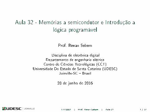
Aula 32 - Memórias a semicondutor e Introdução alógica programável
Prof. Renan Sebem
Disciplina de eletrônica digitalDepartemanto de engenharia elétrica
Centro de Ciências Tecnológicas (CCT)Universidade Do Estado de Santa Catarina (UDESC)
Joinville-SC � Brasil
28 de junho de 2016
ELD0001 ‡ Prof. Renan Sebem ‡ Aula 32 1 / 32
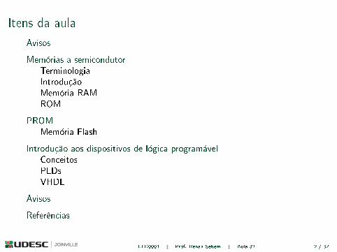
Itens da aula
Avisos
Memórias a semicondutorTerminologiaIntroduçãoMemória RAMROM
PROMMemória Flash
Introdução aos dispositivos de lógica programávelConceitosPLDsVHDL
Avisos
Referências
ELD0001 ‡ Prof. Renan Sebem ‡ Aula 32 2 / 32
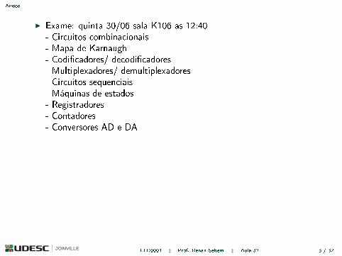
Avisos
I Exame: quinta 30/06 sala K106 as 12:40- Circuitos combinacionais- Mapa de Karnaugh- Codi�cadores/ decodi�cadores- Multiplexadores/ demultiplexadores- Circuitos sequenciais- Máquinas de estados- Registradores- Contadores- Conversores AD e DA
ELD0001 ‡ Prof. Renan Sebem ‡ Aula 32 3 / 32
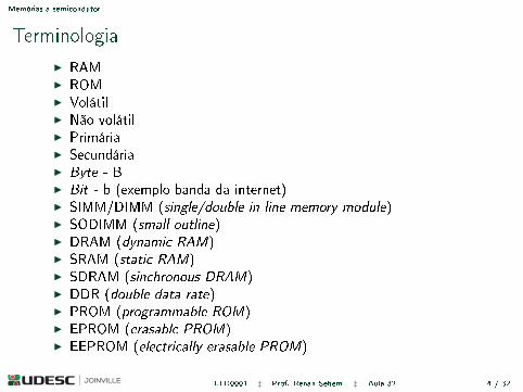
Memórias a semicondutor
Terminologia
I RAMI ROMI VolátilI Não volátilI PrimáriaI SecundáriaI Byte - BI Bit - b (exemplo banda da internet)I SIMM/DIMM (single/double in-line memory module)I SODIMM (small outline)I DRAM (dynamic RAM)I SRAM (static RAM)I SDRAM (sinchronous DRAM)I DDR (double data rate)I PROM (programmable ROM)I EPROM (erasable PROM)I EEPROM (electrically erasable PROM)
ELD0001 ‡ Prof. Renan Sebem ‡ Aula 32 4 / 32
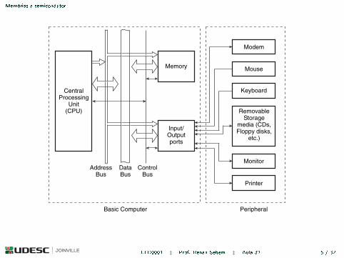
Memórias a semicondutor608 Digital Electronics
Memory
Input/Outputports
CentralProcessing
Unit(CPU)
AddressBus
DataBus
ControlBus
Modem
Mouse
Keyboard
RemovableStorage
media (CDs,Floppy disks,
etc.)
Monitor
Printer
PeripheralDevices
Basic Computer
Figure 15.2 Block diagram of a typical computer system.
complexity of data processing to be done. Special-purpose computers, on the other hand, are designedfor a dedicated application. These computers perform a certain predecided and fixed sequence ofoperations. Typical applications include the computers used for weather forecasting, aircraft controlsystems, missile and other weapon guidance systems, etc.
15.3.2 Classification of Computers on the Basis of the Technology UsedBased on the technology used, the computers are classified as analogue computers, digital computersand hybrid computers. In analogue computers, the input data comprise continuously changing electricalor nonelectrical (temperature, pressure, speed, volume, etc.) information. There are numerous examplesof analogue computational devices. One such device is the speedometer of an automobile. The inputdata to this device or machine are the continuously varying rotational speed of its driveshaft. Therotational motion is converted into a linear movement of a needle pointer that indicates the speedin km/h. A tachometer used to measure the rotational speed is another device of the same type.The input data in the case of a digital computer are discrete in nature. They are represented by abinary notation in the form of 0s and 1s. A hybrid computer is a mixture of the two. It attempts tocombine the good points of both analogue and digital computers. In a typical hybrid computer, themeasuring functions are performed the analogue way while the control and logic functions are digital innature.
ELD0001 ‡ Prof. Renan Sebem ‡ Aula 32 5 / 32
Memórias a semicondutor
I Memória primária:I Registradores de processo, memória principal (RAM - Random Access
Memory), memória cache e memória ROM (Read-only memory);I Tamanhos relativamente pequenos de armazenamento;I Rapidez na transferência de dados;
I Memória secundária:I Discos rígidos (HDD), disco? de estado sólido (SSD), disco
compacto (CD/ DVD), pen drive.I Armazenamento massivo (terabyte);I Transferência de dados mais lenta.
ELD0001 ‡ Prof. Renan Sebem ‡ Aula 32 6 / 32
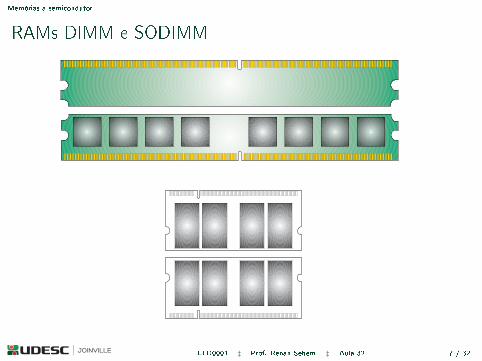
Memórias a semicondutor
RAMs DIMM e SODIMM
Memory Module Specifications
KVR800D2N6/1G1GB 128M x 64-Bit DDR2-800CL6 240-Pin DIMM
Kingston.com Document No. VALUERAM0772-001.A00 04/21/09
DESCRIPTION
This document describes ValueRAM’s 128M x 64-bit 1GB (1024MB) DDR2-800 CL6 SDRAM (Synchronous DRAM) memory module. The components on this module include eight 128M x 8-bit DDR2-800 SDRAM in FBGA packages. This 240-pin DIMM uses gold contact fingers and requires +1.8V. The electrical and mechanical specifications are as follows:
SPECIFICATIONS
Clock Cycle Time (tCK) CL=6 2.5ns (min.) / 8ns (max.)
Row Cycle Time (tRC) 60ns (min.)
Refresh to Active/Refresh 127.5ns Command Time (tRFC)
Row Active Time (tRAS) 45ns (min.) / 70,000ns (max.)
Single Power Supply of +1.8V (+/- .1V)
Power 1.355 W (operating)
UL Rating 94 V - 0
Figure 1: KVR800D2N6/1G 240-Pin DIMM
Note: The module defined in this data sheet is one of several configurations available under this part number. While all configurations are compatible, the DRAM combination and/or the module height may vary from what is described here.
Memory Module Specifications
KVR667D2S5/1G1GB 128M x 64-Bit DDR2-667CL5 200-Pin SODIMM
Kingston.com Document No. VALUERAM0806-001.A00 07/14/09
DESCRIPTION
This document describes ValueRAM’s 128M x 64-bit 1GB (1024MB) CL5 DDR2-667 SDRAM (Synchronous DRAM) memory module. The components on this module include eight 128M x 8-bit DDR2-667 SDRAM in FBGA packages. This 200-pin SODIMM uses gold contact fingers and requires +1.8V. The electrical and mechanical specifications are as follows:
SPECIFICATIONS
Clock Cycle Time (tCK) CL=5 3ns (min.) / 8ns (max.)
Row Cycle Time (tRC) 60ns (min.)
Refresh to Active/Refresh 127.5ns Command Time (tRFC)
Row Active Time (tRAS) 45ns (min.) / 70,000ns (max.)
Single Power Supply of +1.8V (+/- .1V)
Power 1.125 W (operating per module)
UL Rating 94 V - 0
Figure 1: KVR667D2S5/1G 200-Pin SODIMM
Note: The module defined in this data sheet is one of several configurations available under this part number. While all configurations are compatible, the DRAM combination and/or the module height may vary from what is described here.
ELD0001 ‡ Prof. Renan Sebem ‡ Aula 32 7 / 32
Memórias a semicondutor
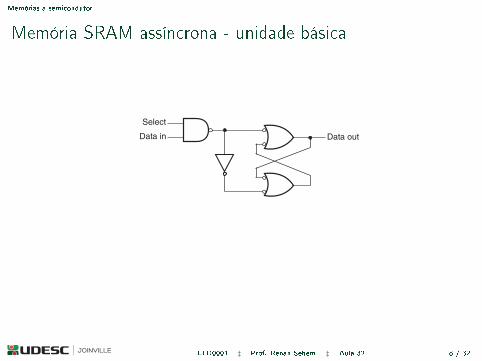
Memória SRAM assíncrona - unidade básica
Computer Fundamentals 613
Select
Data in Data out
Figure 15.4 Basic SRAM memory cell.
SRAMs normally have an address burst feature, which allows the memory to read and write at morethan one location using a single address. Both synchronous and asynchronous SRAMs are availablein bipolar, MOS and BiCMOS technologies. While bipolar SRAM offers a relatively higher speed ofoperation, MOS technology offers a higher capacity and reduced power consumption. Figures 15.5(a)and (b) show the basic bipolar memory cell and the MOS (NMOS more specifically) memory cellrespectively.
15.5.1.1 Asynchronous SRAM
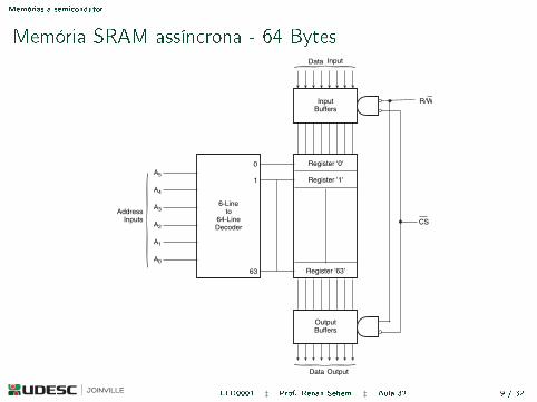
Figure 15.6 shows the typical architecture of a 64×8 asynchronous SRAM. It is capable of storing64 words of eight bits each. The main blocks include a 6-to-64 line address decoder, I/O buffers, 64memory cells and control logic for read/write operations. The memory cells in a row are representedas a register. Each register is an eight-bit register and can be read from as well as written into. Ascan be seen from the figure, all the cells inside the same register share the same decoder output line,also referred to as ‘row line’. The control functions are provided by R/W (read/write) and CS (chipselect) inputs. R/W and CS inputs are also referred to as WE (write enable) and CE (chip enable)inputs respectively. The ‘data input’ and ‘data output’ lines are usually combined by using commoninput/output lines in order to conserve the number of pins on the IC package.
The memory is selected by making CS = 0. During the ‘read’ operation the status of the R/W andCS pins is ‘1’ and ‘0’ respectively, while during the ‘write’ operation it is ‘0’ and ‘0’ respectively.During the ‘read’ operation the input buffers are disabled and the contents of the selected registerappear at the output. During the ‘write’ operation the input buffers are enabled and the output buffersare disabled. The contents of the input buffers are loaded into the selected register, the previous dataof which are overwritten by the new data. The output buffers, being tristate, are in the high-impedancestate during the write operation. CS = 1 deselects the chip, and both the input and the output databuffers get disabled and go to the high-impedance state. The contents of the memory in this caseremain unaffected. ‘Chip select’ inputs are particularly important when more than one RAM memorychip is combined to get a larger memory capacity.
In the case of larger SRAM memories, there are two address decoders, one for rows and one forcolumns. They are referred to as row decoders and column decoders respectively. Some of the addresslines are fed to the row decoder and the rest of the address lines are fed to the column decoder. Figure15.7 shows the architecture of a typical 16K×8 asynchronous SRAM. The memory cells are arrangedin eight arrays of 128 rows and 128 columns each. Memories with a single address decoder are referred
ELD0001 ‡ Prof. Renan Sebem ‡ Aula 32 8 / 32
Memórias a semicondutor
Memória SRAM assíncrona - 64 BytesComputer Fundamentals 615
InputBuffers
Register '0'
Register '1'
Register '63'
OutputBuffers
R/W
CS
6-Lineto
64-LineDecoder
63
0
1A5
A4
A3
A2
A1
A0
AddressInputs
InputData
OutputData
Figure 15.6 Typical architecture of a 64×8 asynchronous SRAM.
The different timing intervals shown in the diagram are defined as follows:
• Complete read cycle time tRC. This is defined as the time interval for which a valid address code isapplied to the address lines during the ‘read’ operation.
• RAM access time tACC. This is defined as the time lapse between the application of a new addressinput and the appearance of valid output data.
• Chip enable access time tCO. This is defined as the time taken by the RAM output to go from theHi-Z state to a valid data level once CS is activated.
• Chip disable access time tOD. This is defined as the time taken by the RAM to return to the Hi-Zstate after CS is deactivated.
ELD0001 ‡ Prof. Renan Sebem ‡ Aula 32 9 / 32
Memórias a semicondutor
Memória SRAM assíncrona - 16 kB616 Digital Electronics
Memory array128 rows
128 columns8 bits
××
R/W
0
AddressLines
Data Input
1 128128
Column Decoder
1
RowDecoder
AddressLines
0
OutputBuffers
DataOutput
CS
Input Buffers
Figure 15.7 Typical architecture of a 16K×8 asynchronous SRAM.
• Complete write cycle time tWC. This is defined as the time interval for which a valid address codeis applied to the address lines during the ‘write’ operation.
• Write pulse width tW. This is the time for which R/W is held LOW during the ‘write’ operation.• Address set-up time tAS.This is the time interval between the appearance of a new address and R/W
going LOW.• Data set-up time tDS. This is defined as the time interval for which the R/W must remain LOW
after valid data are applied to the data inputs.• Data hold time tDH. This is defined as the time interval for which valid input data must remain on
the data lines after the R/W input goes HIGH.• Address hold time interval tAH. This is defined as the time interval for which the valid address must
remain on the address lines after the R/W input goes HIGH.
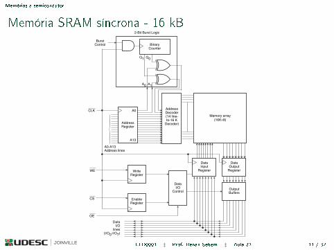
15.5.1.2 Synchronous SRAM
Synchronous SRAM, as mentioned before, is synchronized with the system clock. In the case of acomputer system it operates at the same clock frequency as the microprocessor. This synchronizationof microprocessor and memory ensures faster execution speeds. The basic difference between thearchitecture of synchronous and asynchronous SRAMs is that the synchronous SRAM makes use ofclocked registers to synchronize ‘address’, R/W , CS and ‘data in’ lines to the system clock. Figure15.9 shows the basic architecture of a 32K × 8 synchronous SRAM with a burst feature. As we cansee from the figure, the memory array block, the address decoder block and R/W and CS are the same
ELD0001 ‡ Prof. Renan Sebem ‡ Aula 32 10 / 32
Memórias a semicondutor
Memória SRAM síncrona - 16 kB618 Digital Electronics
BinaryCounter
Q1 Q0
A0 A1
AddressDecoder(14 line-to-16 K
Decoder)AddressRegister
A0
A13
BurstControl
DataOutput
Register
DataInput
Register
OutputBuffers
DataI/O
Control
WriteRegister
EnableRegister
CLK
WE
CS
DataI/O
lines(I/O0-I/O7)
OE
A0-A13Address lines
2-Bit Burst Logic
Memory array(16K 8)×
Figure 15.9 Architecture of a 16K ×8 synchronous SRAM.ELD0001 ‡ Prof. Renan Sebem ‡ Aula 32 11 / 32
Memórias a semicondutor
Memória DRAM - unidade básica
Computer Fundamentals 619
as in the case of an asynchronous SRAM. As mentioned before, most synchronous SRAMs have anaddress burst feature. In this case, when an external address is latched to the address register, a certainnumber of lowest address bits are applied to the burst logic. Burst logic comprises a binary counterand EXCLUSIVE-OR gates. The output of the burst logic, which basically produces a sequence ofinternal addresses, is fed to the address bus decoder. In the case of a two-bit burst logic, the internaladdress sequence generated is given by A1A0, A1A0, A1A0, A1 A0, where A0 and A1 are the addressbits applied to the burst logic. The burst logic shown in Fig. 15.9 is also a two-bit logic.
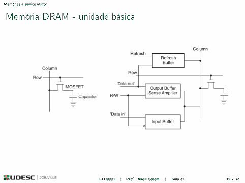
15.5.2 Dynamic RAMThe memory cell in the case of a DRAM comprises a capacitor and a MOSFET. The cell holds a valueof ‘1’ when the capacitor is charged and ‘0’ when it is discharged. The main advantage of this typeof memory is its higher density, or more bits per package, compared with SRAM. This is because thememory cell is very simple compared with that of SRAM. Also, the cost per bit is less in the case ofa DRAM. The disadvantage of this type of memory is the leakage of charge stored on the capacitorsof various memory cells when they are storing a ‘1’. To prevent this from happening, each memorycell in a DRAM needs to be periodically read, its charge (or voltage) compared with a reference valueand then the charge restored to the capacitor. This process is known as ‘memory refresh’ and is doneapproximately every 5–10 ms.
Figure 15.10 shows the basic memory cell of a DRAM and its principle of operation. The MOSFETacts like a switch. When in the ‘write’ mode (R/W = 0!, the input buffers are enabled while theoutput buffers are disabled. When ‘1’ is to be stored in the memory, the ‘data in’ line must be in theHIGH state and the corresponding ‘row line’ should also be in the HIGH state so that the MOSFET isswitched ON. This connects the MOSFET to the ‘data in’ line, and it charges the capacitor to a positivevoltage level. When ‘0’ needs to be stored, the ‘data in’ line is LOW and the capacitor also acquiresthe same level. When the ‘row line’ is taken to the LOW state, the MOSFET is switched OFF and isdisconnected from the bit line. This traps the charge on the capacitor. In ‘read’ mode (R/W = 1!, theoutput buffers are enabled while the input buffers are disabled. When the ‘row line’ is taken to HIGHlogic, the MOSFET is switched ON and connects the capacitor to the ‘data out’ line through the output
Column
MOSFET
Row
Capacitor
RefreshBuffer
Refresh
Output BufferSense Ampliier
'Data out'
Input Buffer
'Data in'
R/W
Row
Column
Figure 15.10 Basic memory cell of a DRAM.
ELD0001 ‡ Prof. Renan Sebem ‡ Aula 32 12 / 32
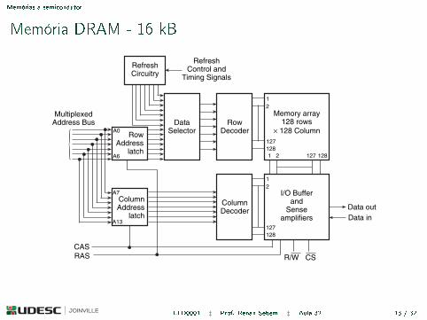
Memórias a semicondutor
Memória DRAM - 16 kB
620 Digital Electronics
buffer. The refresh operation is performed by setting R/W = 1 and by enabling the refresh buffer.There are two basic modes of refreshing the memory, namely the burst refresh and distributed refreshmodes. In burst refresh mode, all rows in the memory array are refreshed consecutively during therefresh burst cycle. In distributed refresh mode, each row is refreshed at intervals interspaced between‘read’ and ‘write’ operations.
15.5.2.1 DRAM Architecture
The architecture of DRAM memory is somewhat different from that of SRAM memory. Row andcolumn address lines are usually multiplexed in a DRAM. This is done to reduce the number ofpins on the package. Row address select (RAS) and column address select (CAS) inputs are used toindicate whether a row or a column is to be addressed. Address multiplexing is particularly attractivefor higher-capacity DRAMs. A 4 MB RAM, for instance, would require 22 address inputs (222 = 4M)"
Figure 15.11 shows the architecture of a 16K × 1 DRAM. The heart of a DRAM is an array of single-bit memory cells. Each cell has a unique position as regards row and column. Other important blocksinclude address decoders (row decoder and column decoder) and refresh control and address latches(row address latch and column address latch). As can be seen from the figure, seven address lines aretime multiplexed at the beginning of the memory cycle by the RAS and CAS lines. Firstly, the seven-bitaddress (A0–A6! is latched into the row address latch, and then the seven-bit address is latched intothe column address latch (A7–A13!. They are then decoded to select the particular memory location.Larger word sizes can be achieved by combining more than one chip. This is discussed in the nextsection. Figures 15.12(a) and (b) respectively show the timing diagrams for read and write operations.A DRAM is relatively slower than a SRAM. The typical access time is in the range 100–250 ns.
DataSelector
RowDecoder
Memory array128 rows128 Column×
12
1271281 2 127 128
ColumnDecoder
I/O Bufferand
Senseamplifiers
12
127128
Data outData in
RowAddress
latch
A0
A6
ColumnAddress
latch
A7
A13
RefreshCircuitry
RefreshControl and
Timing Signals
MultiplexedAddress Bus
R/W CSCASRAS
Figure 15.11 Architecture of a 16K × 1 DRAM.
ELD0001 ‡ Prof. Renan Sebem ‡ Aula 32 13 / 32
Memórias a semicondutor
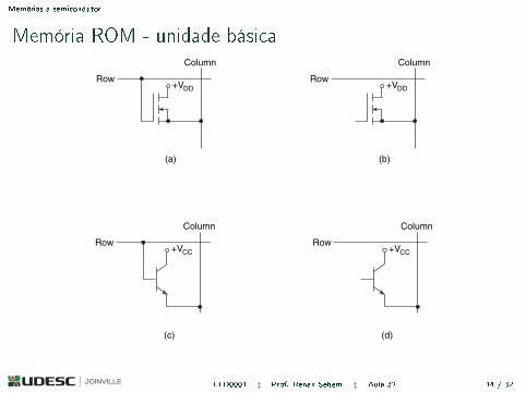
Memória ROM - unidade básica626 Digital Electronics
+VDD
Column
Row
(a)
+VDD
Column
Row
(b)
+VCC
Column
Row
(c)
+VCC
Column
Row
(d)
Figure 15.16 Basic cell connection of a mask-programmed ROM.
In the ROM architecture shown in Fig. 15.17, the number of memory cells in a row represents theword size. The four memory cells in a row here constitute a four-bit register. There are four suchregisters in this ROM. In a 16 × 8 ROM of this type there will be 16 rows of such transistor cells,with each row having eight memory cells. The decoder in that case would be a 1-of-16 decoder.
15.6.2.2 Programmable ROM
In the case of PROMs, instead of being done at the manufacturer’s premises during the manufacturingprocess, the programming is done by the customer with the help of a special gadget called a PROMprogrammer. Since the data, once programmed, cannot be erased and reprogrammed, these devices arealso referred to as one-time programmable ROMs.
The basic memory cell of a PROM is similar to that of a mask-programmed ROM. Figures 15.18(a)and (b) show a MOSFET-based memory cell and bipolar memory cell respectively. In the case of aPROM, each of the connections that were left either intact or open in the case of a mask-programmedROM are made with a thin fusible link, as shown in Fig. 15.18. The different interconnect technologiesused in programmable logic devices are comprehensively covered in Chapter 9. Basic fuse technologiesused in PROMs are metal links, silicon links and PN junctions. These fusible links can be selectivelyblown off to store desired data. A sufficient current is injected through the fusible link to burn itopen to store ‘0’. The programming operation, as said earlier, is done with a PROM programmer. ThePROM chip is plugged into the socket meant for the purpose. The programmer circuitry selects eachaddress of the PROM one by one, burns in the required data and then verifies the correctness of the
ELD0001 ‡ Prof. Renan Sebem ‡ Aula 32 14 / 32
Memórias a semicondutor
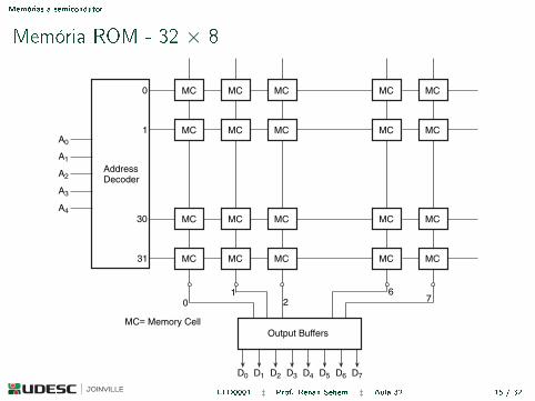
Memória ROM - 32 × 8624 Digital Electronics
AddressDecoder
MCMC MC
MC MCMCMC MC
MC MC0
1A0
MCMC MC
MCMC MC
MC MC30
31
A1
A2
A3
A4
MC MC
Output Buffers
D0 D1 D2 D3 D4 D5 D6 D7
MC= Memory Cell
01
26
7
Figure 15.14 Architecture of 32 × 8 ROM.
known as the access time, tACC. Another useful timing parameter is the output enable time, tOE, whichis the time delay between application of input and appearance of valid data output.
Typical bipolar ROMs have access times of 30–90 ns. In the case of NMOS devices, the accesstimes range from 35 to 500 ns. The output enable time, tOE , in the case of bipolar ROMs is in therange 10–20 ns. For MOS-based ROMs, tOE is in the range 25–100 ns.
15.6.2 Types of ROMDepending upon the methodology of programming, erasing and reprogramming information intoROMs, they are classified as mask-programmed ROMs, programmable ROMs (PROMs) and erasableprogrammable ROMs (EPROMs) [ultraviolet-erasable programmable ROMs (UV EPROMs) andelectrically erasable programmable ROMs (EEPROMs)].
15.6.2.1 Mask-programmed ROM
In the case of a mask-programmed ROM, the ROM is programmed at the manufacturer’s site accordingto the specifications of the customer. A photographic negative, called a mask, is used to store therequired data on the ROM chip. A different mask would be needed for storing each different set
ELD0001 ‡ Prof. Renan Sebem ‡ Aula 32 15 / 32
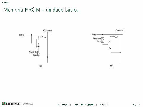
PROM
Memória PROM - unidade básica
628 Digital Electronics
+VDD
Column
Row
(a)
Fusiblelink
(b)
+VCC
Column
Row
Fusiblelink
Figure 15.18 Basic memory cell of a PROM.
15.6.2.3 Erasable PROM
EPROM can be erased and reprogrammed as many times as desired. Once programmed, it is nonvolatile,i.e. it holds the stored data indefinitely. There are two types of EPROM, namely the ultraviolet-erasablePROM (UV EPROM) and electrically erasable PROM (EEPROM).
The memory cell in a UV EPROM is a MOS transistor with a floating gate. In the normal condition,the MOS transistor is OFF. It can be turned ON by applying a programming pulse (in the range 10–25 V)that injects electrons into the floating-gate region. These electrons remain trapped in the gate region evenafter removal of the programming pulse. This keeps the transistor ON once it is programmed to be in thatstate even after the removal of power. The stored information can, however, be erased by exposing thechip to ultraviolet radiation through a transparent window on the top of the chip meant for the purpose.The photocurrent thus produced removes the stored charge in the floating-gate region and brings thetransistor back to the OFF state. The erasing operation takes around 15–20 min, and the process erasesinformation on all cells of the chip. It is not possible to carry out any selective erasure of memorycells. Intel’s 2732 is 4K ×8 UV EPROM hardware implemented with NMOS devices. Type numbers2764, 27128, 27256 and 27512 have capacities of 8K × 8, 16K × 8, 32K × 8 and 64K × 8 respectively.The access time is in the range 150–250 ns. UV EPROMs suffer from disadvantages such as the needto remove the chip from the circuit if it is to be reprogrammed, the nonfeasibility of carrying outselective erasure and the reprogramming process taking several tens of minutes. These are overcomein the EEPROMs and flash memories discussed in the following paragraphs.
The memory cell of an EEPROM is also a floating-gate MOS structure with the slight modificationthat there is a thin oxide layer above the drain of the MOS memory cell. Application of a high-voltageprogramming pulse between gate and drain induces charge in the floating-gate region which can beerased by reversing the polarity of the pulse. Since the charge transport mechanism requires very lowcurrent, erasing and programming operations can be carried out without removing the chip from thecircuit. EEPROMs have another advantage – it is possible to erase and rewrite data in the individualbytes in the memory array. The EEPROMs, however, have lower density (bit capacity per square mmof silicon) and higher cost compared with UV EPROMs.
15.6.2.4 Flash Memory
Flash memories are high-density nonvolatile read/write memories with high density. Flash memorycombines the low cost and high density features of an UV EPROM and the in-circuit electrical
ELD0001 ‡ Prof. Renan Sebem ‡ Aula 32 16 / 32
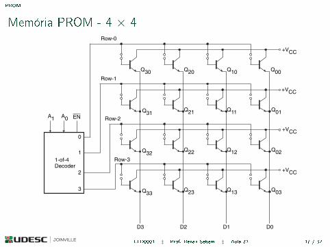
PROM
Memória PROM - 4 × 4Computer Fundamentals 627
Q30 Q20 Q10 Q00
Row-0
Q31Q21 Q11 Q01
Row-1
Q32Q22 Q12 Q02
Row-2
Q33Q23 Q13 Q03
Row-3
+VCC
D3 D2 D1 D0
+VCC
+VCC
+VCC
1-of-4Decoder
1
0
2
3
A1 A0 EN
0011
0101
1100
0011
1011
0010
A1 A0 D3 D2 D1 D0
Address Data
Truth Table
Figure 15.17 Internal structure of a 4 × 4 bipolar mask-programmed ROM.
data before proceeding to the next address. The data are fed to the programmer from a keyboard or adisk drive or from a computer.
PROM chips are available in various word sizes and capacities. 27LS19, 27S21, 28L22, 27S15,24S41, 27S35, 24S81, 27S45, 27S43 and 27S49 are respectively 32 × 8, 256 × 4, 256 × 8, 512 × 8,1K × 4, 1K × 8, 2K × 4, 2K × 8, 4K × 8 and 8K × 8 PROMS. The typical access time in the case ofthese devices is in the range 50–70 ns. MOS PROMs are available with much greater capacities thanbipolar PROMs. Also, the power dissipation is much lower in MOS PROMs than it is in the case ofbipolar PROMs with similar capacities.
ELD0001 ‡ Prof. Renan Sebem ‡ Aula 32 17 / 32
PROM
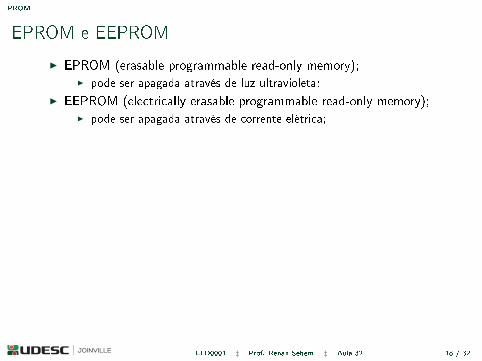
EPROM e EEPROM
I EPROM (erasable programmable read-only memory);I pode ser apagada através de luz ultravioleta;
I EEPROM (electrically erasable programmable read-only memory);I pode ser apagada através de corrente elétrica;
ELD0001 ‡ Prof. Renan Sebem ‡ Aula 32 18 / 32
PROM
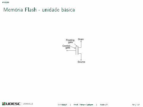
Memória Flash - unidade básica
Computer Fundamentals 629
erasability feature of EEPROM without compromising the high-speed access of both. Structurally, thememory cell of a flash memory is like that of an EPROM. The basic memory cell of a flash memoryis shown in Fig. 15.19. It is a stacked-gate MOSFET with a control gate and floating gate in additionto drain and source. The floating gate stores charge when sufficient voltage is applied to the controlgate. A ‘0’ is stored when there is more charge, and a ‘1’ when there is less charge. The amount ofcharge stored on the floating gate determines whether or not the MOSFET is turned ON.
It is called a flash memory because of its rapid erase and write times. Most flash memory devicesuse a ‘bulk erase’ operation in which all the memory cells on the chip are erased simultaneously. Someflash memory devices offer a ‘sector erase’ mode in which specific sectors of the memory devicecan be erased at a time. This mode comes in handy when only a portion of the memory needs to beupdated.
Figure 15.20 shows the basic array of a 4 × 4 flash memory. As in the case of earlier memories,there is an address decoder that selects the row. During the read operation, for a cell containing a‘1’ there is current through the bit line which produces a voltage drop across the active load. This iscompared with the reference voltage, and the output bit is ‘1’. If the memory cell has a ‘0’, there isvery little current in the bit line. Memory sticks are flash memories. They are available in 4, 8, 16, 32,64 and 128 MB sizes.
To sum up, while PROMs are least complex and low cost, they cannot be erased and reprogrammed.UV EPROMs are a little more complex and costly, but then they can be erased and reprogrammed bybeing taken out of the circuit. Flash memories are in-circuit electrically erasable either sectorwise or inbulk mode. The most complex and most expensive are the EEPROMs, but then they offer byte-by-byteelectrical erasability in circuit.
15.6.3 Applications of ROMsThe majority of ROM applications originate from the need for nonvolatile storage of data or programcodes. Some of the common application areas include firmware, bootstrap memory, look-up tables,function generators and auxiliary memory.
The most common application of ROM chips is in the storage of data and program codes thatmust be made available to microprocessor-based systems such as microcomputers on power-up. Thiscomponent of the software is referred to as firmware as it comes embedded in the hardware with themachine. Even consumer products such as CD players, microwave ovens, washing machines, etc., haveembedded microcontrollers that have a microprocessor to control and monitor the operation accordingto the information stored on the ROM.
Source
DrainFloatinggate
Controlgate
Figure 15.19 Basic cell of flash memory.
ELD0001 ‡ Prof. Renan Sebem ‡ Aula 32 19 / 32
PROM
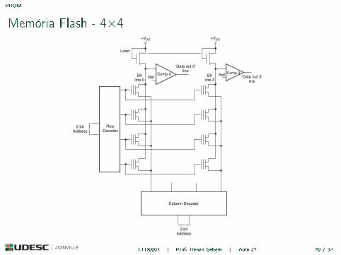
Memória Flash - 4×4630 Digital Electronics
'Data out 0'line
Bitline 0
'Data out 3'line
Bitline 3
+VDD
Comp 3Comp 0Ref
Load
RowDecoder
2 bitAddress
2 bitAddress
Column Decoder
Ref
+VDD
Figure 15.20 Basic array of 4 × 4 flash memory.
ROMs are also used to store the ‘bootstrap program’ in computers. It is a relatively small programcontaining instructions that will cause the CPU to initialize the system hardware after it is powered on.The bootstrap program then loads the operating system programs stored in the secondary memory intoits main internal memory. The computer then begins to execute the operating system program. Thisstart-up operation is also called the ‘booting operation’.
ROMs are frequently used as ‘look-up tables’. There are two sets of data, one constituting theaddress and the other corresponding to the data stored in various memory locations of the ROM.Corresponding to each address input, there is a unique data ouput. One typical application is that of
ELD0001 ‡ Prof. Renan Sebem ‡ Aula 32 20 / 32
Introdução aos dispositivos de lógica programável
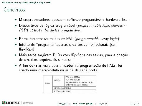
Conceitos
I Microprocessadores possuem software programável e hardware �xo;I Dispositivos de lógica programável (programmable logic devices -
PLD) possuem hardware programável.
I Primeiramente chamados de PAL (programmable array logic);I Intuito de "programar"apenas circuitos combinacionais (sem
�ip-�ops);I Mais tarde surgiram PLDs com �ip-�ops nas saídas, para a criação
de circuitos sequênciais simples;I A �m de criar mais possibilidades na programação de PALs, foi
criado uma macro-célula na saída de cada porta.468 CHAPTER 18 Programmable Logic Devices
PLD, and GAL/PALCE) are now collectively referred to as SPLDs (simple PLDs). Of these, GAL is the only one still manufactured.
In the mid 1980s, several GAL devices were fabricated on the same chip using a sophisticated routing scheme, more advanced silicon technology, and several additional features, like JTAG support (port for circuit access/test defi ned by the Joint Test Action Group and specifi ed in the IEEE 1149.1 standard) and interface to several logic standards. Such an approach became known as CPLD (complex PLD). CPLDs are currently very popular due to their relatively high density, high performance, and low cost (some cost nearly as low as $1), making them a popular choice in many applications, including consumer elec-tronics, computers, automotive, etc.
Finally, also in the mid 1980s, FPGAs (fi eld programmable gate arrays) were introduced. FPGAs differ from CPLDs in architecture, technology, built-in features, and cost. They target mainly complex, large-size, top-performance designs, like gigabit transceivers, high-complexity switching, HDTV, wireless, and other telecommunication applications.
A fi nal remark is that CPLDs are essentially nonvolatile, while FPGAs are volatile. CPLDs normally employ EEPROM (Section 17.5) or fl ash memory (Section 17.6) to store the interconnects, while FPGAs employ SRAM (Section 16.2). Consequently, the latter needs a confi guration nonvolatile memory from which the program is loaded at power up. A table illustrating the evolution of PLDs is presented in Figure 18.1.
18.2 SPLDsAs mentioned above, PAL, PLA, and GAL devices are collectively called SPLDs, which stands for simple PLDs. A description of each one of these architectures follows.
18.2.1 PAL DevicesPAL (programmable array logic) chips were introduced by Monolithic Memories in the mid 1970s. Its basic architecture is illustrated in Figure 18.2, where the little ovals represent programmable connec-tions. As can be seen, the circuit is composed of a programmable array of AND gates followed by a fi xed array of OR gates. This implementation is based on the fact that any combinational function can be represented by a sum-of-products (SOP), as seen in Section 5.3. The products are computed by the AND gates, while the sum is computed by the OR gate that follows.
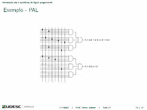
A PAL-based example is depicted in Figure 18.3, which computes the combinational functions f1 = a � b + a� � b� � c� � d� + b � d and f2 = a � b � c + d. The dark ovals indicate a connection. The outputs of non-programmed AND gates are set to zero.
As mentioned earlier, the main limitation of this approach is that it is appropriate only for the imple-mentation of combinational functions. To circumvent this problem, registered PALs were launched toward
FIGURE 18.1. Summary of PLD evolution.
ELD0001 ‡ Prof. Renan Sebem ‡ Aula 32 21 / 32
Introdução aos dispositivos de lógica programável
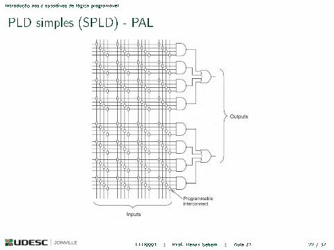
PLD simples (SPLD) - PAL18.2 SPLDs 469
FIGURE 18.2. Basic PAL architecture.
FIGURE 18.3. PAL-based example where two combinational functions (f1, f2) of four variables (a, b, c, d ) are implemented. Dark ovals indicate a connection. The output of a nonprogrammed AND gate is set to zero.
ELD0001 ‡ Prof. Renan Sebem ‡ Aula 32 22 / 32
Introdução aos dispositivos de lógica programável
Exemplo - PAL
18.2 SPLDs 469
FIGURE 18.2. Basic PAL architecture.
FIGURE 18.3. PAL-based example where two combinational functions (f1, f2) of four variables (a, b, c, d ) are implemented. Dark ovals indicate a connection. The output of a nonprogrammed AND gate is set to zero.
ELD0001 ‡ Prof. Renan Sebem ‡ Aula 32 23 / 32
Introdução aos dispositivos de lógica programável
PLD simples (SPLD) - PLA
470 CHAPTER 18 Programmable Logic Devices
the end of the 1970s. These included a fl ip-fl op at each output (after each OR gate in Figure 18.2), thus allowing the construction of sequential circuits as well (though only very simple ones).
An example of a then popular PAL chip is the PAL16L8 device, which contained 16 inputs and eight outputs (though only 18 I/O pins were available because it was a 20-pin DIP package with two pins destined to the power supply, plus 10 IN pins, two OUT pins, and six IN/OUT pins). Its registered coun-terpart was the 16R8 device.
The early technology employed in the fabrication of PALs was bipolar (Chapter 8) with fuses or anti-fuses normally employed to establish the (nonvolatile) array connections. They operated with a 5 V sup-ply voltage and exhibited a large power consumption for such small devices (around 200 mA with open outputs) with a maximum frequency around 100 MHz.
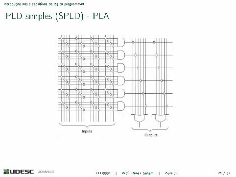
18.2.2 PLA DevicesPLA (programmable logic array) chips were introduced in the mid 1970s by Signetics. The basic archi-tecture of a PLA is illustrated in Figure 18.4. Comparing it to that in Figure 18.2, we observe that the only fundamental difference between them is that while a PAL has programmable AND connections and fi xed OR connections, both are programmable in a PLA. The obvious advantage is greater fl exibility because more combinational functions (more product terms) can be implemented with the same amount of hardware. On the other hand, the extra propagation delay introduced by the additional program-mable interconnections lowered their speed.
An example of a then popular PLA chip is the Signetics PLS161 device. It contained 12 inputs and eight outputs, with a total of 48 12-input AND gates, followed by a total of eight 48-input OR gates. At the outputs, additional programmable XOR gates were also available.
FIGURE 18.4. Basic PLA architecture.
ELD0001 ‡ Prof. Renan Sebem ‡ Aula 32 24 / 32
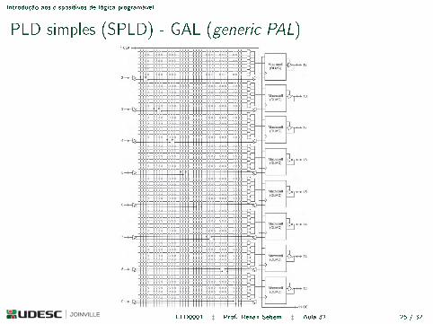
Introdução aos dispositivos de lógica programável
PLD simples (SPLD) - GAL (generic PAL)472 CHAPTER 18 Programmable Logic Devices
The Xilinx XC9500 CPLD series is an example of a CPLD constructed according to the general archi-tecture depicted in Figure 18.7 (and the same is true for the CoolRunner family, though this employs PLAs instead of GALs). It contains n PLDs, each resembling a V18 GAL (therefore similar to the 16V8 architecture of Figure 18.5, but with 18 programmable AND arrays instead of eight, hence with 18 macro-cells each), where n = 2, 4, 6, 8, 12, or 16. With these values of n, CPLDs with 18n = 36 up to 288 macrocells are obtained. This fact can be verifi ed in the XC9500 data sheets available at www.xilinx.com.
FIGURE 18.5. GAL 16V8 chip. ELD0001 ‡ Prof. Renan Sebem ‡ Aula 32 25 / 32
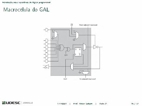
Introdução aos dispositivos de lógica programável
Macrocélula do GAL
FIGURE 18.6. Macrocell diagram.
FIGURE 18.7. Basic CPLD architecture, which consists of n PLDs (GALs, in general) interconnected through a programmable switch array, plus I/O bank and clock/control unit.
18.3 CPLDs 473
ELD0001 ‡ Prof. Renan Sebem ‡ Aula 32 26 / 32
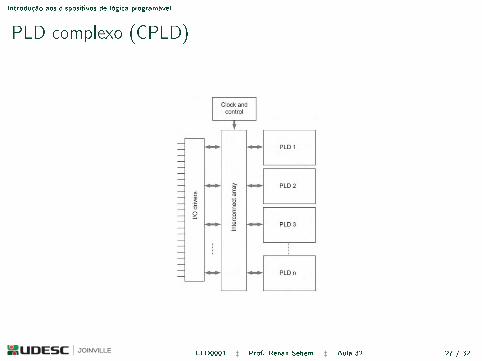
Introdução aos dispositivos de lógica programável
PLD complexo (CPLD)FIGURE 18.6. Macrocell diagram.
FIGURE 18.7. Basic CPLD architecture, which consists of n PLDs (GALs, in general) interconnected through a programmable switch array, plus I/O bank and clock/control unit.
18.3 CPLDs 473
ELD0001 ‡ Prof. Renan Sebem ‡ Aula 32 27 / 32
Introdução aos dispositivos de lógica programável
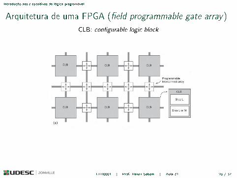
Arquitetura de uma FPGA (�eld programmable gate array)
CLB: con�gurable logic block
Another improvement, which was adopted in the Stratix III FPGA, consists of using strained silicon (described in Section 9.8) to increase the transistors’ speed. All Stratix III transistors are strained, allowing many of them to be constructed with midox instead of thinox, thus preventing leakage without compro-mising speed.
18.4.2 FPGA ArchitectureThe overall architecture of FPGAs is depicted in Figure 18.12, which presents a simplifi ed view of the Virtex 5 and Stratix III FPGAs. The former is illustrated in Figure 18.12(a), where the programmable logic blocks are called CLB (confi gurable logic block), with each CLB composed of two Slices (one of type L,
FIGURE 18.12. Simplifi ed FPGA architectures: (a) Xilinx Virtex 5; (b) Altera Stratix III. Additional blocks (SRAM, DSP, etc.) and additional routing not shown.
18.4 FPGAs 479
ELD0001 ‡ Prof. Renan Sebem ‡ Aula 32 28 / 32
Introdução aos dispositivos de lógica programável
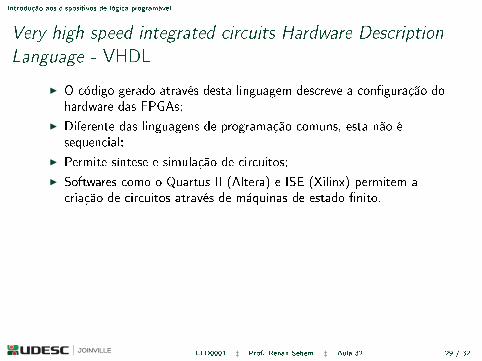
Very high speed integrated circuits Hardware Description
Language - VHDL
I O código gerado através desta linguagem descreve a con�guração dohardware das FPGAs;
I Diferente das linguagens de programação comuns, esta não ésequencial;
I Permite síntese e simulação de circuitos;I Softwares como o Quartus II (Altera) e ISE (Xilinx) permitem a
criação de circuitos através de máquinas de estado �nito.
ELD0001 ‡ Prof. Renan Sebem ‡ Aula 32 29 / 32

Avisos
I Exame: quinta 30/06 sala K106 as 12:40- Circuitos combinacionais- Mapa de Karnaugh- Codi�cadores/ decodi�cadores- Multiplexadores/ demultiplexadores- Circuitos sequenciais- Máquinas de estados- Registradores- Contadores- Conversores AD e DA
ELD0001 ‡ Prof. Renan Sebem ‡ Aula 32 30 / 32
Referências
[1] Ivan V. Idoeta and Francisco Gabriel Capuano. Elementos deEletrônica Digital. São Paulo: Érica, 2014.
[2] Anil K. Maini. Digital Electronics Principles: Devices andApplications. Wiley, 2007.
[3] Ronald J. Tocci. Sistemas Digitais � Princípios e Aplicações. PrenticeHall, 2001.
ELD0001 ‡ Prof. Renan Sebem ‡ Aula 32 31 / 32
Aula 32 - Memórias a semicondutor e Introdução alógica programável
Prof. Renan Sebem
Disciplina de eletrônica digitalDepartemanto de engenharia elétrica
Centro de Ciências Tecnológicas (CCT)Universidade Do Estado de Santa Catarina (UDESC)
Joinville-SC � Brasil
28 de junho de 2016
Obrigado.
ELD0001 ‡ Prof. Renan Sebem ‡ Aula 32 32 / 32