aalborg universitet dual converter fed open-end ... · ˚ vector representing the flux linkage.! i...
TRANSCRIPT
Aalborg Universitet
Dual Converter Fed Open-End Transformer Topology with Parallel Converters andIntegrated Magnetics
Gohil, Ghanshyamsinh Vijaysinh; Bede, Lorand; Teodorescu, Remus; Kerekes, Tamas;Blaabjerg, FredePublished in:I E E E Transactions on Industrial Electronics
DOI (link to publication from Publisher):10.1109/TIE.2016.2548999
Publication date:2016
Document VersionEarly version, also known as pre-print
Link to publication from Aalborg University
Citation for published version (APA):Gohil, G. V., Bede, L., Teodorescu, R., Kerekes, T., & Blaabjerg, F. (2016). Dual Converter Fed Open-EndTransformer Topology with Parallel Converters and Integrated Magnetics. I E E E Transactions on IndustrialElectronics, 63(8), 4929 - 4941. https://doi.org/10.1109/TIE.2016.2548999
General rightsCopyright and moral rights for the publications made accessible in the public portal are retained by the authors and/or other copyright ownersand it is a condition of accessing publications that users recognise and abide by the legal requirements associated with these rights.
? Users may download and print one copy of any publication from the public portal for the purpose of private study or research. ? You may not further distribute the material or use it for any profit-making activity or commercial gain ? You may freely distribute the URL identifying the publication in the public portal ?
Take down policyIf you believe that this document breaches copyright please contact us at [email protected] providing details, and we will remove access tothe work immediately and investigate your claim.
IEEE TRANSACTIONS ON INDUSTRIAL ELECTRONICS
Dual Converter Fed Open-End TransformerTopology with Parallel Converters and Integrated
Magnetics
Ghanshyamsinh Gohil, Student Member, IEEE, Lorand Bede, Student Member, IEEE, RemusTeodorescu, Fellow, IEEE, Tamas Kerekes, Senior Member, IEEE, and Frede Blaabjerg, Fellow, IEEE
Abstract—A converter system for high power applica-tions, connected to a medium-voltage network using a step-up transformer, is presented in this paper. The converter-side winding of the transformer is configured as an open-end and both the ends of the windings are fed from two dif-ferent converter groups. Each converter group comprisesof two parallel Voltage Source Converters (VSCs), whosecarrier signals are interleaved to improve the harmonicquality of the resultant switched output voltage of that con-verter group. However, an additional inductive componentis required to suppress the circulating current that flowsbetween the parallel interleaved VSCs. An integrated induc-tor is proposed which suppresses the circulating currentin both the converter groups. In addition, the functionalityof the line filter inductor is also integrated. Flux in variousparts of the integrated inductor is analyzed and a designprocedure is also described. The volume and the lossesof the proposed solution are compared with that of thestate-of-art solution. The control of the proposed convertersystem is also discussed. The analysis has been verified bythe simulation and experimental results.
Index Terms—Voltage source converters (VSC), parallel,interleaving, dual converter, open-end transformer, windpower, integrated inductor, magnetic integration, wind en-ergy conversion system
NOMENCLATURE−→φ Vector representing the flux linkage.−→Ic Vector representing the circulating current.−→Ir Vector representing the resultant current.−→I Vector representing the leg currents of phase x.−→Vp Switched output voltage vector.−→Vv Voltage vector, representing the potential of the com-
mon points of the HSCG and the LSCG.−→V Coil voltage vector.Lc Circulating current inductance matrix.µ0 Permeability of the air.−→V ∗H Reference voltage space vector for HSCG.−→V ∗L Reference voltage space vector for LSCG.φblmax Maximum value of the flux in the bridge legs.φlmax Maximum value of the flux in the limbs.
Manuscript received August 3, 2015; revised December 09, 2015 andFebruary 04, 2016; accepted March 08, 2016. This work was supportedby the Innovation Foundation Denmark through the Intelligent EfficientPower Electronics (IEPE) technology platform.
The authors are with the Department of Energy Technology, AalborgUniversity, 9220 Aalborg East, Denmark (e-mail: [email protected]).
φx,k Total flux linking k coil of phase x.φxby
Flux in a bottom yoke.φxcy
Flux in a common yoke.φxk,cmax
Maximum value of the circulating flux component.φxk,c
Circulating flux component that links with the kth coilof phase x.
φxk,fFundamental frequency component of the flux thatlinks with the kth coil of phase x.
φxtyFlux in a top yoke.
φymaxMaximum value of the flux in top and bottom yokes.
ψH Reference voltage space vector angle for HSCG.ψL Reference voltage space vector angle for LSCG.ψmax voltage space vector angle for which the circulating
flux component achieves its maximum value.<l Reluctance of a limb.<y Reluctance of the top, bottom, and common yoke.<bl Reluctance of a bridge leg.<g′1 Equivalent reluctance of an air gap g1.<g′2 Equivalent reluctance of an air gap g2.θ Displacement power factor angle.A
′
g Effective cross-section area of the air gap.Aw Window area.Acl Cross section area of limb.Acu Cross section area of the coil conductor.Bml
Permissible value of the flux density in the limb.Bmy Permissible value of the flux density in the yoke.Bmbl
Permissible value of the flux density in the bridge leg.Cd Damping capacitor.Cf Shunt capacitive branch of the LCL filter.Ir Rated current.Ix Resultant line current.IxH
Resultant line current of the high-side converter group.Ixk
Leg current of phase x of the k VSC.IxL
Resultant line current of the low-side converter group.IxH,c
Circulating current between the parallel interleavedVSCs of the high-side converter group.
IxL,cCirculating current between the parallel interleavedVSCs of the low-side converter group.
J Current density.Ks Stacking Factor.Kw Window utilization factor.Lc Circulating current inductance.Lf Line filter inductance.
IEEE TRANSACTIONS ON INDUSTRIAL ELECTRONICS
Lg Grid-side inductor of the LCL filter.lg1 Air gap length between the cell and the bridge leg.lg2 Length of the air gap in the cell structure.M Modulation index, defined as the ratio of the peak of
the reference signal to the half of the dc-link voltage.N Number of turns.Rd Damping resistor.S VA rating of the converter.Ts Switching interval.Vx Resultant phase voltage.VxHoH Resultant voltage of high-side converter group.VxLoL Resultant voltage of low-side converter group.Vph Rated phase voltage.VxkoH Switched output voltage of phase x of kth VSC with
respect to the oH .VxkoL Switched output voltage of phase x of kth VSC with
respect to the oL.Vxs
Resultant switched output voltage of phase x.VxC,f
Voltage across the filter capacitor.x Subscript, which represents phases a, b, and c.
I. INTRODUCTION
FOR the high power applications, the current can be re-duced by using a medium voltage converter. A three-level
neutral point diode clamped (3L-NPC) topology is commonlyused [1]. However, an extra control efforts are required tobalance the dc-link capacitor voltage [2]. Moreover, the semi-conductor loss distribution is unequal [3] and this may lead tothe de-rating of the Voltage Source Converter (VSC) [4]. Onthe other hand, the two-level VSC is used extensively in manyindustrial applications due to its simple power circuitry andproven technology. Therefore, it is highly desirable to realizethe medium voltage converter system using the standard two-level VSC.
Many grid-connected applications use transformer betweenthe converter system and the grid for matching the voltagelevels. Also in some applications, the grid codes demandgalvanic isolation. In such systems, the primary winding canbe configured as an open-end winding and can be fed fromboth the ends using two-level VSCs [5]. The number of levelsin the output voltage is same as that of the 3L-NPC and eachof the two-level VSC operates with the half of the dc-linkvoltage than that of the 3L-NPC. However, common-mode(CM) circulating current flows through the closed path if boththe VSCs are connected to the common dc-link. But in manyapplications, isolated dc-links can be readily derived from thesource itself and such extra measures for the CM circulatingcurrent suppression may not be required. For example, theisolated dc-links can be obtained in
1) PhotoVoltaic (PV) systems by dividing the total numberof arrays into two groups to form separate dc-links [5].
2) Wind Energy Conversion System (WECS): isolated dc-links can be obtained using the dual stator-winding gen-erator [6].Therefore, the analysis presented in this paper is mainlyfocused on the dual converter fed open-end transformer
topology with two separate dc-links.
Phase cPhase b
Phase a
High-sideconverter
group
Low-sideconverter
group
Integratedinductor
VdcH2
VdcH2
VdcL2
VdcL2Ia1
Ia3Ia4
Ia2
IaHIaL
Ia,g
a1
a3oH oL
Cf
aH aL
a2
a4
MV GridPCC
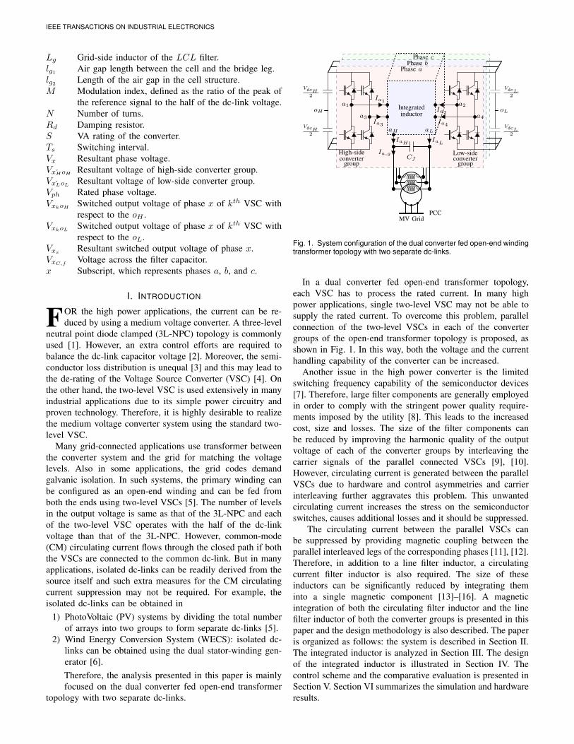
Fig. 1. System configuration of the dual converter fed open-end windingtransformer topology with two separate dc-links.
In a dual converter fed open-end transformer topology,each VSC has to process the rated current. In many highpower applications, single two-level VSC may not be able tosupply the rated current. To overcome this problem, parallelconnection of the two-level VSCs in each of the convertergroups of the open-end transformer topology is proposed, asshown in Fig. 1. In this way, both the voltage and the currenthandling capability of the converter can be increased.
Another issue in the high power converter is the limitedswitching frequency capability of the semiconductor devices[7]. Therefore, large filter components are generally employedin order to comply with the stringent power quality require-ments imposed by the utility [8]. This leads to the increasedcost, size and losses. The size of the filter components canbe reduced by improving the harmonic quality of the outputvoltage of each of the converter groups by interleaving thecarrier signals of the parallel connected VSCs [9], [10].However, circulating current is generated between the parallelVSCs due to hardware and control asymmetries and carrierinterleaving further aggravates this problem. This unwantedcirculating current increases the stress on the semiconductorswitches, causes additional losses and it should be suppressed.
The circulating current between the parallel VSCs canbe suppressed by providing magnetic coupling between theparallel interleaved legs of the corresponding phases [11], [12].Therefore, in addition to a line filter inductor, a circulatingcurrent filter inductor is also required. The size of theseinductors can be significantly reduced by integrating theminto a single magnetic component [13]–[16]. A magneticintegration of both the circulating filter inductor and the linefilter inductor of both the converter groups is presented in thispaper and the design methodology is also described. The paperis organized as follows: the system is described in Section II.The integrated inductor is analyzed in Section III. The designof the integrated inductor is illustrated in Section IV. Thecontrol scheme and the comparative evaluation is presented inSection V. Section VI summarizes the simulation and hardwareresults.
IEEE TRANSACTIONS ON INDUSTRIAL ELECTRONICS
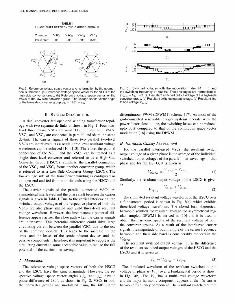
TABLE IPHASE SHIFT BETWEEN THE CARRIER SIGNALS
Converter VSC1 VSC2 VSC3 VSC4
Phase shift 0 90 180 270
−−→VH1
−−→VH2
−−→VH3
−−→VH4
−−→VH5
−−→VH6
−→V ∗H
ψH
(a)
−−→VL1
−−→VL2
−−→VL3
−−→VL4
−−→VL5
−−→VL6
−→V ∗L
ψL
(b)
Fig. 2. Reference voltage space vector and its formation by the geomet-rical summation. (a) Reference voltage space vector for the VSCs of thehigh-side converter group, (b) Reference voltage space vector for theVSCs of the low-side converter group. The voltage space vector angleof the low-side converter group ψL = 180 + ψH .
II. SYSTEM DESCRIPTION
A dual converter fed open-end winding transformer topol-ogy with two separate dc-links is shown in Fig. 1. Four two-level three phase VSCs are used. Out of these four VSCs,VSC1 and VSC3 are connected in parallel and share the samedc-link. The carrier signals of these two parallel two-levelVSCs are interleaved. As a result, three-level resultant voltagewaveforms can be achieved [10], [13]. Therefore, the parallelconnection of the VSC1 and the VSC3 can be treated as asingle three-level converter and referred to as a High-SideConverter Group (HSCG). Similarly, the parallel connectionof the VSC2 and VSC4 forms another converter group, whichis referred to as a Low-Side Converter Group (LSCG). Thelow-voltage side of the transformer winding is configured asan open-end and fed from both the ends using the HSCG andthe LSCG.
The carrier signals of the parallel connected VSCs aresymmetrical interleaved and the phase shift between the carriersignals is given in Table I. Due to the carrier interleaving, theswitched output voltages of the respective phases of both theVSCs are also phase shifted and yield three-level resultantvoltage waveform. However, the instantaneous potential dif-ference appears across the close path when the carrier signalsare interleaved. This potential difference could drive largecirculating current between the parallel VSCs due to the useof the common dc-link. This leads to the increase in thestress and the losses of the semiconductor devices and thepassive components. Therefore, it is important to suppress thecirculating current to some acceptable value to realize the fullpotential of the carrier interleaving.
A. Modulation
The reference voltage space vectors of both the HSCGand the LSCG have the same magnitude. However, the re-spective voltage space vector angles (ψH and ψL) have aphase difference of 180, as shown in Fig. 2. VSCs in boththe converter groups are modulated using the 60 clamp
−0.4−0.2
00.20.4
V´
xH
oH
(a)
−0.50
0.5
Vxs
(b)
−1−0.5
00.51
Vasbs
(c)
Fig. 3. Switched voltages with the modulation index M = 1 andthe switching frequency of 750 Hz, These voltages are normalized to(VdcH + VdcL )/2. (a) Resultant switched output voltage of the high-sideconverter group, (b) Resultant switched output voltage, (c) Resultant lineto line voltage Vasbs .
discontinuous PWM (DPWM1) scheme [17]. As most of thegrid-connected renewable energy systems operate with thepower factor close to one, the switching losses can be reducedupto 50% compared to that of the continuous space vectormodulation [18] using the DPWM1.
B. Harmonic Quality AssessmentFor the parallel interleaved VSCs, the resultant switch
output voltage of a given phase is the average of the individualswitched output voltages of the parallel interleaved legs of thatphase and for the HSCG, it is given as
VxHoH =Vx1oH + Vx3oH
2(1)
Similarly, the resultant output voltage of the LSCG is givenas
VxLoL =Vx2oL + Vx4oL
2(2)
The simulated resultant voltage waveform of the HSCG overa fundamental period is shown in Fig. 3(a), which exhibitsthree-level voltage waveforms. The closed form theoreticalharmonic solution for resultant voltage for asymmetrical reg-ular sampled DPWM1 is derived in [10] and it is used toobtain the harmonic spectra of the resultant voltage of boththe converter groups. As a result of the interleaved carriersignals, the magnitude of odd multiple of the carrier frequencyharmonic and their side band is considerably reduced in theVxHoH .
The resultant switched output voltage Vxsis the difference
of the resultant switched output voltages of the HSCG and theLSCG and it is given as
Vxs = VxHoH − VxLoL (3)
The simulated waveform of the resultant switched outputvoltage of phase a (Vas ) over a fundamental period is shownin Fig. 3(b). The Vas has a multi-level voltage waveformand the major harmonic component appears at the 4th carrierharmonic frequency component. The resultant switched output
IEEE TRANSACTIONS ON INDUSTRIAL ELECTRONICS
A B
C
DE
FG
H
Cell (phase a)Cell (phase b)
Cell (phase c)
Coil b2
Coil c2
Coil b1
Coil c1Air gaps lg
Coil a3
Coil a1
Coil a4
Coil a2
Bridge legs
Bridge legs
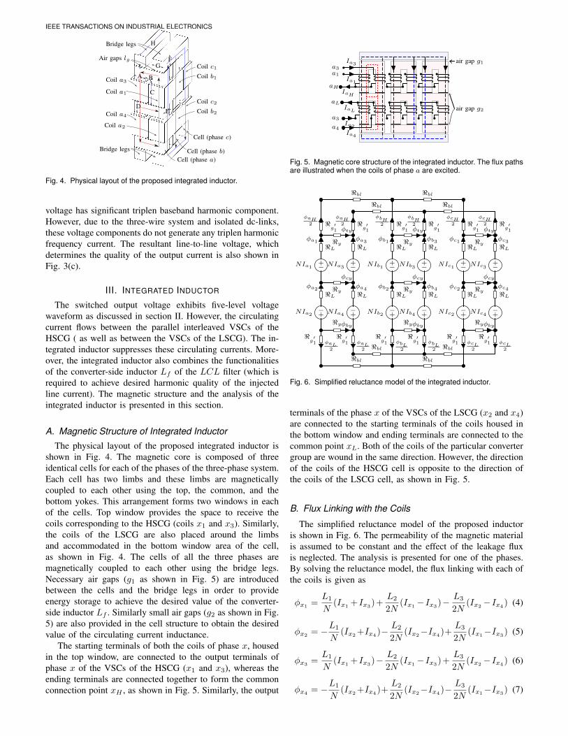
Fig. 4. Physical layout of the proposed integrated inductor.
voltage has significant triplen baseband harmonic component.However, due to the three-wire system and isolated dc-links,these voltage components do not generate any triplen harmonicfrequency current. The resultant line-to-line voltage, whichdetermines the quality of the output current is also shown inFig. 3(c).
III. INTEGRATED INDUCTOR
The switched output voltage exhibits five-level voltagewaveform as discussed in section II. However, the circulatingcurrent flows between the parallel interleaved VSCs of theHSCG ( as well as between the VSCs of the LSCG). The in-tegrated inductor suppresses these circulating currents. More-over, the integrated inductor also combines the functionalitiesof the converter-side inductor Lf of the LCL filter (which isrequired to achieve desired harmonic quality of the injectedline current). The magnetic structure and the analysis of theintegrated inductor is presented in this section.
A. Magnetic Structure of Integrated Inductor
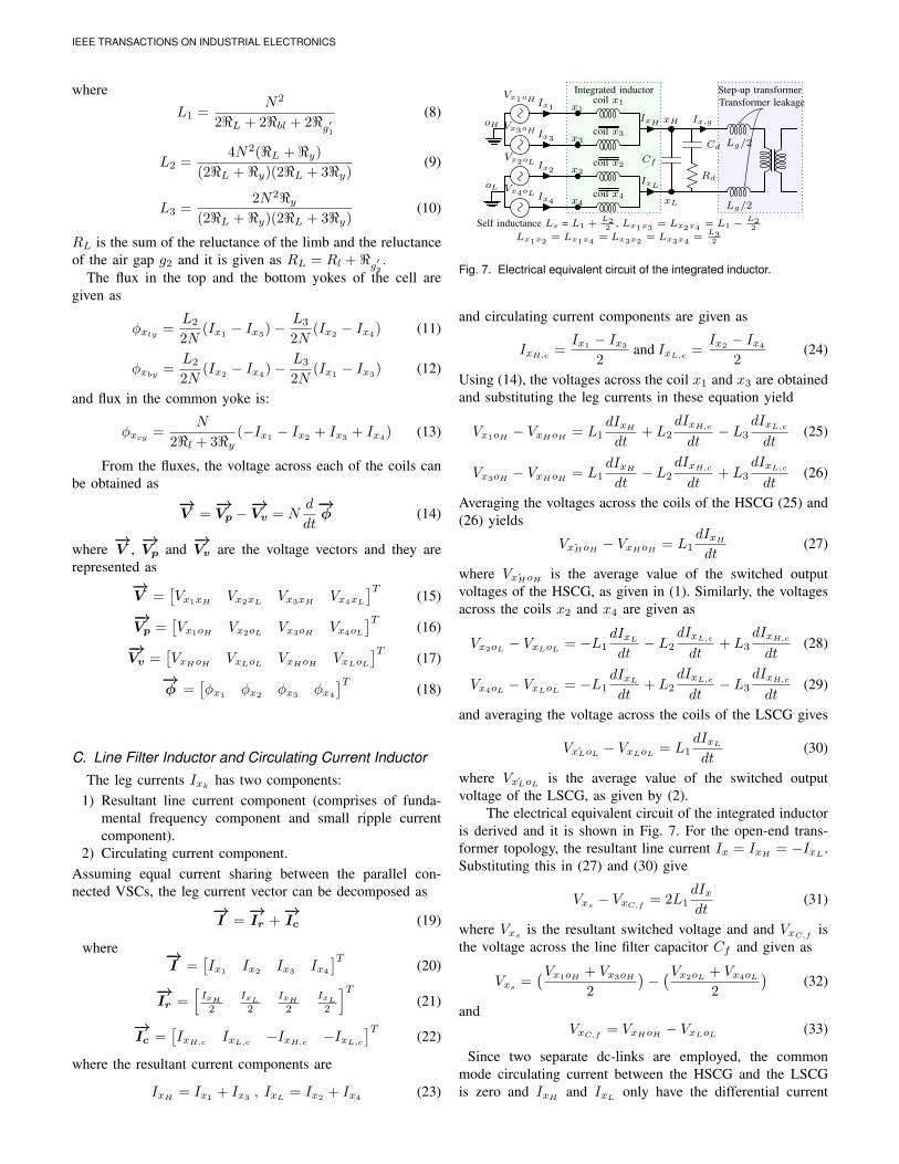
The physical layout of the proposed integrated inductor isshown in Fig. 4. The magnetic core is composed of threeidentical cells for each of the phases of the three-phase system.Each cell has two limbs and these limbs are magneticallycoupled to each other using the top, the common, and thebottom yokes. This arrangement forms two windows in eachof the cells. Top window provides the space to receive thecoils corresponding to the HSCG (coils x1 and x3). Similarly,the coils of the LSCG are also placed around the limbsand accommodated in the bottom window area of the cell,as shown in Fig. 4. The cells of all the three phases aremagnetically coupled to each other using the bridge legs.Necessary air gaps (g1 as shown in Fig. 5) are introducedbetween the cells and the bridge legs in order to provideenergy storage to achieve the desired value of the converter-side inductor Lf . Similarly small air gaps (g2 as shown in Fig.5) are also provided in the cell structure to obtain the desiredvalue of the circulating current inductance.
The starting terminals of both the coils of phase x, housedin the top window, are connected to the output terminals ofphase x of the VSCs of the HSCG (x1 and x3), whereas theending terminals are connected together to form the commonconnection point xH , as shown in Fig. 5. Similarly, the output
a1a3
aH
a3
a4
aL
air gap g1
air gap g2
Ia1
Ia3
IaH
Ia2
Ia4
IaL
Fig. 5. Magnetic core structure of the integrated inductor. The flux pathsare illustrated when the coils of phase a are excited.
+−NIa1
<L
φa1
<g′1
φaH2
<L
φa2
+−NIa2
<g′1 φaL
2
+−NIa3
<L
φa3
<g′1
φaH2
<L
φa4
+−NIa4
<g′1 φaL
2
+−NIb1
<L
φb1
<g′1
φbH2
<L
φb2
+−NIb2
<g′1 φbL
2
+−NIb3
<L
φb3
<g′1
φbH2
<L
φb4
+−NIb4
<g′1 φbL
2
+−NIc1
<L
φc1
<g′1
φcH2
<L
φc2
+−NIc2
<g′1 φcL
2
+−NIc3
<L
φc3
<g′1
φcH2
<L
φc4
+−NIc4
<g′1 φcL
2
<y
φcy
<y
φty
<yφby
<y
φcy
<y
φty
<yφby
<y
φcy
<y
φty
<yφby
<bl <bl
<bl <bl
<bl <bl
<bl <bl
Fig. 6. Simplified reluctance model of the integrated inductor.
terminals of the phase x of the VSCs of the LSCG (x2 and x4)are connected to the starting terminals of the coils housed inthe bottom window and ending terminals are connected to thecommon point xL. Both of the coils of the particular convertergroup are wound in the same direction. However, the directionof the coils of the HSCG cell is opposite to the direction ofthe coils of the LSCG cell, as shown in Fig. 5.
B. Flux Linking with the Coils
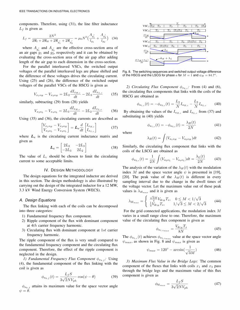
The simplified reluctance model of the proposed inductoris shown in Fig. 6. The permeability of the magnetic materialis assumed to be constant and the effect of the leakage fluxis neglected. The analysis is presented for one of the phases.By solving the reluctance model, the flux linking with each ofthe coils is given as
φx1=L1
N(Ix1
+Ix3)+
L2
2N(Ix1
−Ix3)− L3
2N(Ix2
−Ix4) (4)
φx2= −L1
N(Ix2
+Ix4)− L2
2N(Ix2
−Ix4)+
L3
2N(Ix1
−Ix3) (5)
φx3=L1
N(Ix1
+Ix3)− L2
2N(Ix1
−Ix3)+
L3
2N(Ix2
−Ix4) (6)
φx4 = −L1
N(Ix2+Ix4)+
L2
2N(Ix2−Ix4)−
L3
2N(Ix1−Ix3) (7)
IEEE TRANSACTIONS ON INDUSTRIAL ELECTRONICS
where
L1 =N2
2<L + 2<bl + 2<g′1(8)
L2 =4N2(<L + <y)
(2<L + <y)(2<L + 3<y)(9)
L3 =2N2<y
(2<L + <y)(2<L + 3<y)(10)
RL is the sum of the reluctance of the limb and the reluctanceof the air gap g2 and it is given as RL = Rl + <g′2 .
The flux in the top and the bottom yokes of the cell aregiven as
φxty=
L2
2N(Ix1
− Ix3)− L3
2N(Ix2
− Ix4) (11)
φxby=
L2
2N(Ix2
− Ix4)− L3
2N(Ix1
− Ix3) (12)
and flux in the common yoke is:
φxcy =N
2<l + 3<y(−Ix1 − Ix2 + Ix3 + Ix4) (13)
From the fluxes, the voltage across each of the coils canbe obtained as
−→V =
−→Vp −
−→Vv = N
d
dt
−→φ (14)
where−→V ,
−→Vp and
−→Vv are the voltage vectors and they are
represented as−→V =
[Vx1xH
Vx2xLVx3xH
Vx4xL
]T(15)
−→Vp =
[Vx1oH Vx2oL Vx3oH Vx4oL
]T(16)
−→Vv =
[VxHoH VxLoL VxHoH VxLoL
]T(17)
−→φ =
[φx1
φx2φx3
φx4
]T(18)
C. Line Filter Inductor and Circulating Current InductorThe leg currents Ixk
has two components:1) Resultant line current component (comprises of funda-
mental frequency component and small ripple currentcomponent).
2) Circulating current component.Assuming equal current sharing between the parallel con-nected VSCs, the leg current vector can be decomposed as
−→I =
−→Ir +
−→Ic (19)
where −→I =
[Ix1 Ix2 Ix3 Ix4
]T(20)
−→Ir =
[IxH
2
IxL
2
IxH
2
IxL
2
]T(21)
−→Ic =
[IxH,c
IxL,c−IxH,c
−IxL,c
]T(22)
where the resultant current components are
IxH= Ix1
+ Ix3, IxL
= Ix2+ Ix4
(23)
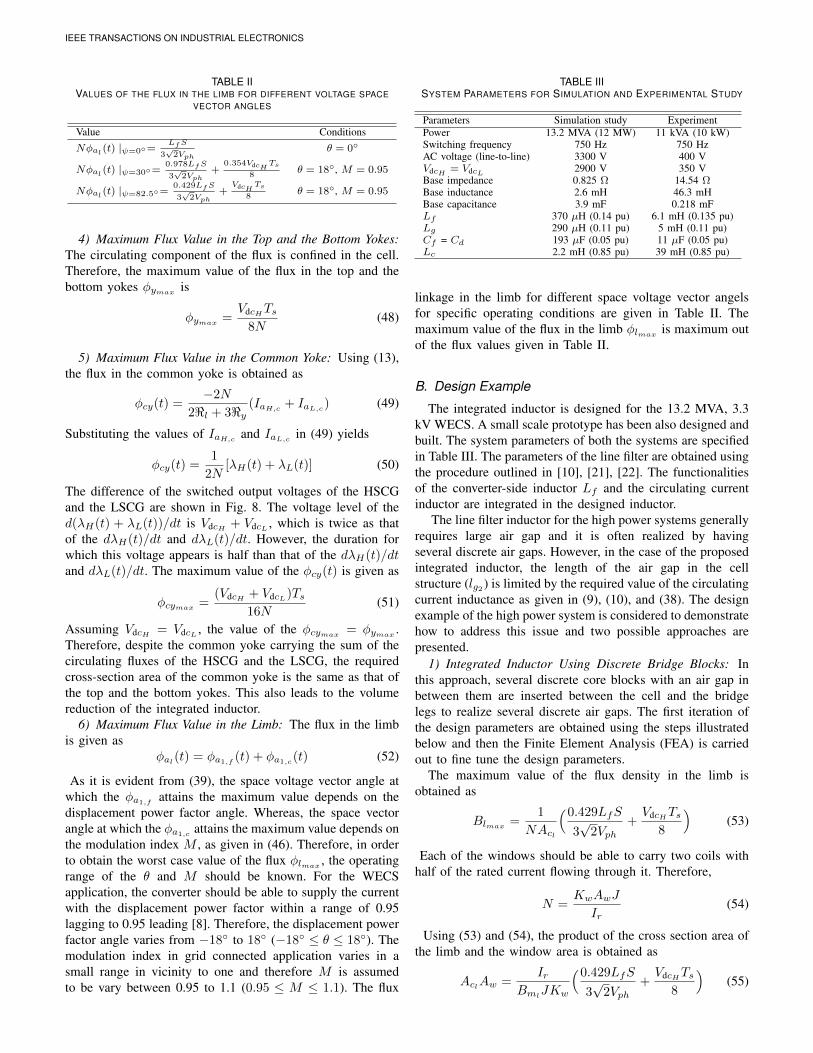
Integrated inductor Step-up transformerTransformer leakage
Vx1oH Ix1coil x1
Vx3oH Ix3coil x3
Vx2oL Ix2coil x2
Vx4oL Ix4coil x4
oL
oH
Cf
Cd
Rd
Lg/2
Lg/2
x1
x3
x2
x4
xH
xL
IxH
IxL
Ix,g
Self inductance Ls = L1 +L22 , Lx1x3
= Lx2x4= L1 − L2
2
Lx1x2= Lx1x4
= Lx3x2= Lx3x4
=L32
Fig. 7. Electrical equivalent circuit of the integrated inductor.
and circulating current components are given as
IxH,c=Ix1 − Ix3
2and IxL,c
=Ix2 − Ix4
2(24)
Using (14), the voltages across the coil x1 and x3 are obtainedand substituting the leg currents in these equation yield
Vx1oH − VxHoH = L1dIxH
dt+ L2
dIxH,c
dt− L3
dIxL,c
dt(25)
Vx3oH − VxHoH = L1dIxH
dt− L2
dIxH,c
dt+ L3
dIxL,c
dt(26)
Averaging the voltages across the coils of the HSCG (25) and(26) yields
VxHoH − VxHoH = L1dIxH
dt(27)
where VxHoH is the average value of the switched outputvoltages of the HSCG, as given in (1). Similarly, the voltagesacross the coils x2 and x4 are given as
Vx2oL − VxLoL = −L1dIxL
dt− L2
dIxL,c
dt+ L3
dIxH,c
dt(28)
Vx4oL − VxLoL = −L1dIxL
dt+ L2
dIxL,c
dt− L3
dIxH,c
dt(29)
and averaging the voltage across the coils of the LSCG gives
VxLoL − VxLoL = L1dIxL
dt(30)
where VxLoL is the average value of the switched outputvoltage of the LSCG, as given by (2).
The electrical equivalent circuit of the integrated inductoris derived and it is shown in Fig. 7. For the open-end trans-former topology, the resultant line current Ix = IxH
= −IxL.
Substituting this in (27) and (30) give
Vxs− VxC,f
= 2L1dIxdt
(31)
where Vxsis the resultant switched voltage and and VxC,f
isthe voltage across the line filter capacitor Cf and given as
Vxs=
(Vx1oH + Vx3oH
2
)−(Vx2oL + Vx4oL
2
)(32)
andVxC,f
= VxHoH − VxLoL (33)
Since two separate dc-links are employed, the commonmode circulating current between the HSCG and the LSCGis zero and IxH
and IxLonly have the differential current
IEEE TRANSACTIONS ON INDUSTRIAL ELECTRONICS
components. Therefore, using (31), the line filter inductanceLf is given as
Lf =2N2
2<l + 2<bl + 2<g′1+ 2<
g′2
= µ0N2(Ag′1lg1
+Ag′2
lg2
)(34)
where Ag′1 and Ag′2are the effective cross-section area of
an air gaps g1 and g2, respectively and it can be obtained byevaluating the cross-section area of the air gap after addinglength of the air gap to each dimension in the cross-section.
For the parallel interleaved VSCs, the switched outputvoltages of the parallel interleaved legs are phase shifted andthe difference of these voltages drives the circulating current.Using (25) and (26), the difference of the switched outputvoltages of the parallel VSCs of the HSCG is given as
Vx1oH − Vx3oH = 2L2
dIxH,c
dt− 2L3
dIxL,c
dt(35)
similarly, subtracting (29) from (28) yields
Vx2oL − Vx4oL = 2L3
dIxH,c
dt− 2L2
dIxL,c
dt(36)
Using (35) and (36), the circulating currents are described as[Vx1oH − Vx3oH
Vx2oL − Vx4oL
]= Lc
d
dt
[IxH,c
IxL,c
](37)
where Lc is the circulating current inductance matrix andgiven as
Lc =
[2L2 −2L3
−2L3 2L2
](38)
The value of Lc should be chosen to limit the circulatingcurrent to some acceptable limits.
IV. DESIGN METHODOLOGY
The design equations for the integrated inductor are derivedin this section. The design methodology is also illustrated bycarrying out the design of the integrated inductor for a 12 MW,3.3 kV Wind Energy Conversion System (WECS).
A. Design EquationsThe flux linking with each of the coils can be decomposed
into three categories:1) Fundamental frequency flux component.2) Ripple component of the flux with dominant component
at 4th carrier frequency harmonic.3) Circulating flux with dominant component at 1st carrier
frequency harmonic.The ripple component of the flux is very small compared tothe fundamental frequency component and the circulating fluxcomponent. Therefore, the effect of the ripple component isneglected in the design.
1) Fundamental Frequency Flux Component φxk,f: Using
(4), the fundamental component of the flux linking with thecoil is given as
φak,f(t) =
LfS
3√2NVph
cos(ψ − θ) (39)
φak,fattains its maximum value for the space vector angle
ψ = θ.
TsVSC1
VSC3λH
T0 T3 T2 T2 T3 T0
T2 T3 T0 T0 T3 T2
dλHdt
VSC2 T5 T5 T6 T7 T7 T6
λL
VSC4 T5 T5T6 T7 T7 T6
dλLdt
d(λH+λL)
dt
λH + λL
Fig. 8. The switching sequences and switched output voltage differenceof the HSCG and the LSCG for phase a for M = 1 and ψH = 84.7.
2) Circulating Flux Component φxk,c: From (4) and (6),
the circulating flux components that links with the coils of theHSCG are obtained as
φa1,c(t) = −φa3,c(t) =L2
NIaH,c
− L3
NIaL,c
(40)
By obtaining the values of the IaH,cand IaL,c
from (37) andsubstituting in (40) yields
φa1,c(t) = −φa3,c(t) =λH(t)
2N(41)
whereλH(t) =
∫(Va1oH − Va3oH )dt (42)
Similarly, the circulating flux component that links with thecoils of the LSCG are obtained as
φa2,c(t) =1
2N
∫(Va2oL − Va4oL)dt =
λL(t)
2N(43)
The analysis of the variation of the λH(t) with the modulationindex M and the space vector angle ψ is presented in [19],[20]. The peak value of the λH(t) is different in everysampling interval due to the change in the dwell times ofthe voltage vector. Let the maximum value out of these peakvalues is λHmax
and it is given as
λHmax =
√3M4 VdcHTs, 0 ≤M < 1/
√3
14VdcHTs, 1/
√3 ≤M < 2/
√3
(44)
For the grid connected applications, the modulation index Mvaries in a small range close to one. Therefore, the maximumvalue of the circulating flux component is given as
φa1,cmax=VdcHTs8N
(45)
The φa1,c(t) achieves φa1,cmaxvalue at the space vector angle
ψmax, as shown in Fig. 8 and ψmax is given as
ψmax = 120 − arcsin(1√3M
) (46)
3) Maximum Flux Value in the Bridge Legs: The commoncomponent of the fluxes that links with coils x1 and x3 passthrough the bridge legs and the maximum value of this fluxcomponent is given as
φblmax=
LfS
3√2NVph
(47)
IEEE TRANSACTIONS ON INDUSTRIAL ELECTRONICS
TABLE IIVALUES OF THE FLUX IN THE LIMB FOR DIFFERENT VOLTAGE SPACE
VECTOR ANGLES
Value Conditions
Nφal (t) |ψ=0=LfS
3√
2Vphθ = 0
Nφal (t) |ψ=30=0.978LfS
3√
2Vph+
0.354VdcHTs
8θ = 18, M = 0.95
Nφal (t) |ψ=82.5=0.429LfS
3√2Vph
+VdcH
Ts
8θ = 18, M = 0.95
4) Maximum Flux Value in the Top and the Bottom Yokes:The circulating component of the flux is confined in the cell.Therefore, the maximum value of the flux in the top and thebottom yokes φymax is
φymax =VdcHTs8N
(48)
5) Maximum Flux Value in the Common Yoke: Using (13),the flux in the common yoke is obtained as
φcy(t) =−2N
2<l + 3<y(IaH,c
+ IaL,c) (49)
Substituting the values of IaH,cand IaL,c
in (49) yields
φcy(t) =1
2N[λH(t) + λL(t)] (50)
The difference of the switched output voltages of the HSCGand the LSCG are shown in Fig. 8. The voltage level of thed(λH(t) + λL(t))/dt is VdcH + VdcL , which is twice as thatof the dλH(t)/dt and dλL(t)/dt. However, the duration forwhich this voltage appears is half than that of the dλH(t)/dtand dλL(t)/dt. The maximum value of the φcy(t) is given as
φcymax =(VdcH + VdcL)Ts
16N(51)
Assuming VdcH = VdcL , the value of the φcymax= φymax
.Therefore, despite the common yoke carrying the sum of thecirculating fluxes of the HSCG and the LSCG, the requiredcross-section area of the common yoke is the same as that ofthe top and the bottom yokes. This also leads to the volumereduction of the integrated inductor.
6) Maximum Flux Value in the Limb: The flux in the limbis given as
φal(t) = φa1,f (t) + φa1,c(t) (52)
As it is evident from (39), the space voltage vector angle atwhich the φa1,f attains the maximum value depends on thedisplacement power factor angle. Whereas, the space vectorangle at which the φa1,c attains the maximum value depends onthe modulation index M , as given in (46). Therefore, in orderto obtain the worst case value of the flux φlmax , the operatingrange of the θ and M should be known. For the WECSapplication, the converter should be able to supply the currentwith the displacement power factor within a range of 0.95lagging to 0.95 leading [8]. Therefore, the displacement powerfactor angle varies from −18 to 18 (−18 ≤ θ ≤ 18). Themodulation index in grid connected application varies in asmall range in vicinity to one and therefore M is assumedto be vary between 0.95 to 1.1 (0.95 ≤ M ≤ 1.1). The flux
TABLE IIISYSTEM PARAMETERS FOR SIMULATION AND EXPERIMENTAL STUDY
Parameters Simulation study ExperimentPower 13.2 MVA (12 MW) 11 kVA (10 kW)Switching frequency 750 Hz 750 HzAC voltage (line-to-line) 3300 V 400 VVdcH = VdcL 2900 V 350 VBase impedance 0.825 Ω 14.54 ΩBase inductance 2.6 mH 46.3 mHBase capacitance 3.9 mF 0.218 mFLf 370 µH (0.14 pu) 6.1 mH (0.135 pu)Lg 290 µH (0.11 pu) 5 mH (0.11 pu)Cf = Cd 193 µF (0.05 pu) 11 µF (0.05 pu)Lc 2.2 mH (0.85 pu) 39 mH (0.85 pu)
linkage in the limb for different space voltage vector angelsfor specific operating conditions are given in Table II. Themaximum value of the flux in the limb φlmax
is maximum outof the flux values given in Table II.
B. Design Example
The integrated inductor is designed for the 13.2 MVA, 3.3kV WECS. A small scale prototype has been also designed andbuilt. The system parameters of both the systems are specifiedin Table III. The parameters of the line filter are obtained usingthe procedure outlined in [10], [21], [22]. The functionalitiesof the converter-side inductor Lf and the circulating currentinductor are integrated in the designed inductor.
The line filter inductor for the high power systems generallyrequires large air gap and it is often realized by havingseveral discrete air gaps. However, in the case of the proposedintegrated inductor, the length of the air gap in the cellstructure (lg2 ) is limited by the required value of the circulatingcurrent inductance as given in (9), (10), and (38). The designexample of the high power system is considered to demonstratehow to address this issue and two possible approaches arepresented.
1) Integrated Inductor Using Discrete Bridge Blocks: Inthis approach, several discrete core blocks with an air gap inbetween them are inserted between the cell and the bridgelegs to realize several discrete air gaps. The first iteration ofthe design parameters are obtained using the steps illustratedbelow and then the Finite Element Analysis (FEA) is carriedout to fine tune the design parameters.
The maximum value of the flux density in the limb isobtained as
Blmax=
1
NAcl
(0.429LfS3√2Vph
+VdcHTs
8
)(53)
Each of the windows should be able to carry two coils withhalf of the rated current flowing through it. Therefore,
N =KwAwJ
Ir(54)
Using (53) and (54), the product of the cross section area ofthe limb and the window area is obtained as
AclAw =Ir
BmlJKw
(0.429LfS3√2Vph
+VdcHTs
8
)(55)
IEEE TRANSACTIONS ON INDUSTRIAL ELECTRONICS
TABLE IVPARAMETERS OF THE DESIGNED INTEGRATED INDUCTOR. SEE FIG. 4
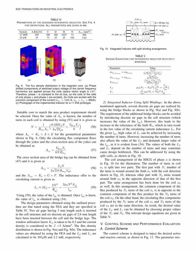
FOR DEFINITIONS. ALL PARAMETERS ARE GIVEN IN MM.
System A,B,E,F,G C D H N Acu (mm2)12 MW 205 300 180 1025 14 40010 kW 25 75 25 25 104 2.62
(a) (b) (c)
Fig. 9. The flux density distribution in the magnetic core. (a) Phaseshifted components of switched output voltage of the carrier frequencyharmonics are applied across the coils (space vector angle is 240.Therefore, phase c is clamped to the dc bus, so the coils of the cellsof only phase a and phase b are excited), (b) Coils are excited with thecommon component of the current (Iak = 1600 A, Ibk = Ick =-800A),(c) Photograph of the implemented inductor for a 11 kVA prototype.
Suitable core to match the area product requirement shouldbe selected. Once the value of Acl is known, the number ofturns in each coil is obtained by using (53) and it is given as
N =1
BmlAcl
(0.429LfS3√2Vph
+VdcHTs
8
)(56)
where Acl = Ks × A × E for the geometrical parametersshown in Fig. 4. Only the circulating flux component flowsthrough the yokes and the cross-section area of the yokes canbe obtained as
Acy =VdcHTs8NBmy
(57)
The cross section area of the bridge leg can be obtained from(47) and it is given as
Acbl =LfS
3√2NBmbl
Vph(58)
and the Acbl = Ks × G × F . The inductance offer to thecirculating current is given as
Lc ≈ 2L2 =2N2
<g′2=
2µ0N2Ag′2
lg2(59)
Using (59), the value of the lg2 is obtained. Once lg2 is know,the value of lg1 is obtained using (34).
The design parameters obtained using the outlined proce-dure are fine tuned using the FEA and they are specified inTable IV. Two air gaps having 3 mm length each is insertedin the cell structure and six discrete air gaps of 2.6 mm lengthhave been inserted between the cell and the bridge legs. Thewindow utilization factor Kw is taken to be 0.3 and the currentdensity is considered to be J =3 A/mm2. The flux densitydistribution is shown in Fig. 9(a) and Fig. 9(b). The inductancevalues are obtained by using the FEA and the Lf and Lc arecalculated to be 395µH and 2.2 mH, respectively.
air gap g1Bridge leg
air gaps g2 x x x
Coil a1N1 turnsN2 turns
N1 turns
N2 turnsCoil a3
Fig. 10. Integrated inductor with split winding arrangement.
TABLE VDESIGN EQUATIONS FOR INTEGRATED INDUCTOR WITH SPLIT
WINDINGS
Parameter Value
φak,fmax= φblmax
LfS
3√2(N1−N2)Vph
φa1,cmax= φymax
VdcHTs
8(N1+N2)
φcymax
(VdcH+VdcL
)Ts
16(N1+N2)
Lf µ0(N1 −N2)2(Ag
′1
lg1+A
g′2
lg2
)Lc
2lg2
µ0(N1 +N2)2Ag′2
2) Integrated Inductor Using Split Windings: In the abovementioned approach, several discrete air gaps are realized byusing the bridge blocks as shown in Fig. 9(a) and Fig. 9(b).The requirement of the additional bridge blocks can be avoidedby introducing discrete air gaps in the cell structure (whichincreases the value of the lg2 ). However, this leads to theincrease in the reluctance of the limb <L, which in turn resultin the low value of the circulating current inductance Lc. Forthe given lg2 , high value of Lc can be achieved by increasingthe number of turns. However, increasing the number of turnsalso affects the value of the Lf and demands larger value ofthe lg1 , as it is evident from (34). The values of both the Lfand Lc depend on the number of turns and may sometimecause design bottleneck. This can be addressed by using thesplit coils, as shown in Fig. 10.
The coil arrangement of the HSCG of phase a is shownin Fig. 10 for the illustration. The number of turns in coila1 is split into two parts. The first part with N1 number ofthe turns is wound around the limb a1 with the coil directionshown in Fig. 10, whereas other part with N2 turns woundaround limb a3 in the opposite direction of that of the firstpart. The same arrangement has been done for the coil a3as well. In this arrangement, the common component of theflux produced by N1 turns of the coil a1 is in opposite to thecommon component of the flux produce by the N2 turns ofthe coil a3. On the other hand, the circulating flux componentsproduced by the N1 turns of the coil a1 and N2 turns of thecoil a3 are in the same direction. As result, the desired valueof the Lf and Lc can be obtained by choosing proper valuesof the N1 and N2. The relevant design equations are given inTable V.
V. CONTROL SCHEME AND PERFORMANCE EVALUATION
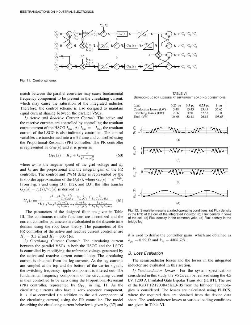
A. Control SchemeThe control scheme is designed to inject the desired active
and reactive current, as shown in Fig. 11. The parameter mis-
IEEE TRANSACTIONS ON INDUSTRIAL ELECTRONICS
abcαβ
IαIβ
+-
I∗α, I∗β
GPR(s) abcαβIaH
IbHIcH
++Ia1Ib1Ic1
-+Ia3Ib3Ic3
X0.5
IaH,cIbH,cIcH,c
abcαβ0
+-
0
GPR(s)αβ0
abc
++
-+
V ∗a1
,V ∗b1
,V ∗c1
V ∗a3
,V ∗b3
,V ∗c3
Ia2Ib2Ic2
Ia4Ib4Ic4
+- X
0.5IaL,cIbL,cIcL,c abc
αβ0+-
0
GPR(s)αβ0
abc
++
-+
-1 X V ∗a2
,V ∗b2
,V ∗c2
V ∗a4
,V ∗b4
,V ∗c4
Fig. 11. Control scheme.
match between the parallel converter may cause fundamentalfrequency component to be present in the circulating current,which may cause the saturation of the integrated inductor.Therefore, the control scheme is also designed to maintainequal current sharing between the parallel VSCs.
1) Active and Reactive Current Control: The active andthe reactive currents are controlled by controlling the resultantoutput current of the HSCG IaH . As IaH = −IaL , the resultantcurrent of the LSCG is also indirectly controlled. The controlvariables are transformed into a αβ frame and controlled usingthe Proportional-Resonant (PR) controller. The PR controlleris represented as GPR(s) and it is given as
GPR(s) = Kp + kis
s2 + ω20
(60)
where ω0 is the angular speed of the grid voltage and kpand ki are the proportional and the integral gain of the PRcontroller. The control and PWM delay is represented by thefirst order approximation of the Gd(s), where Gd(s) = e−
sTs4 .
From Fig. 7 and using (31), (32), and (33), the filter transferGf (s) = Ix(s)/Vx(s) is derived as
Gf (s)=1
sLf
s3+s2Cf+Cd
CfCdRd+s 1
LgCf+ 1LgCfCdRd
s3+s2Cf+Cd
CfCdRd+s
Lf+Lg
LfLgCf+
Lf+Lg
LfLgCfCdRd
(61)
The parameters of the designed filter are given in TableIII. The continuous transfer functions are discretized and thecurrent controller parameters are calculated in the discrete timedomain using the root locus theory. The parameters of thePR controller of the active and reactive current controller areKp = 3.1 Ω and Ki = 605 Ω/s.
2) Circulating Current Control: The circulating currentbetween the parallel VSCs in both the HSCG and the LSCGis controlled by modifying the reference voltage generated bythe active and reactive current control loop. The circulatingcurrent is obtained from the leg currents. As the leg currentsare sampled at the top and the bottom of the carrier signals,the switching frequency ripple component is filtered out. Thefundamental frequency component of the circulating currentis then controlled to be zero using the Proportional-Resonant(PR) controller, represented by GPRc
in Fig. 11. As thecirculating currents also have a zero sequence component,it is also controlled (in addition to the αβ component ofthe circulating current) using the PR controller. The modeldescribing the circulating current behavior is given by (37) and
TABLE VISEMICONDUCTOR LOSSES AT DIFFERENT LOADING CONDITIONS
Load 0.25 pu 0.5 pu 0.75 pu 1 puConduction losses (kW) 5.48 13.43 23.45 35.65Switching losses (kW) 20.6 39.0 52.67 70.0Total (kW) 26.08 52.43 76.12 105.65
−101
Bl
(T)
(a)
−101
By
(T)
(b)
−101
Bcy
(T)
(c)
−101
Bbl
(T)
(d)
Fig. 12. Simulation results at rated operating conditions. (a) Flux densityin the limb of the cell of the integrated inductor, (b) Flux density in yokeof the cell, (c) Flux density in the common yoke, (d) Flux density in thebridge leg.
it is used to derive the controller gains, which are obtained askpc = 8.22 Ω and kic = 4305 Ω/s.
B. Loss Evaluation
The semiconductor losses and the losses in the integratedinductor are evaluated in this section.
1) Semiconductor Losses: For the system specificationsconsidered in this study, the VSCs can be realized using the 4.5kV, 1200 A Insulated Gate Bipolar Transistor (IGBT). The useof the IGBT FZ1200R45KL3-B5 from the Infineon Technolo-gies is considered. The losses are calculated using PLECS,where the required data are obtained from the device datasheet. The semiconductor losses at various loading conditionsare given in Table VI.
IEEE TRANSACTIONS ON INDUSTRIAL ELECTRONICS
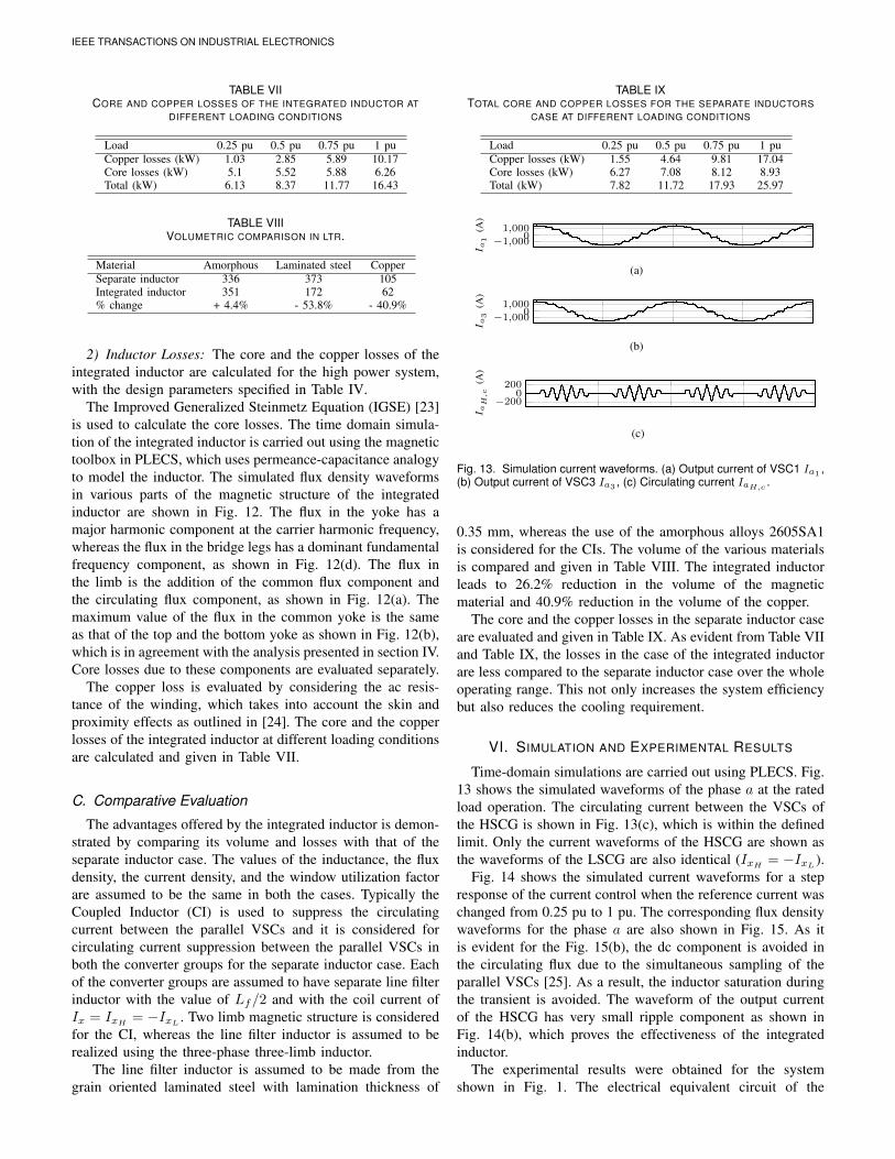
TABLE VIICORE AND COPPER LOSSES OF THE INTEGRATED INDUCTOR AT
DIFFERENT LOADING CONDITIONS
Load 0.25 pu 0.5 pu 0.75 pu 1 puCopper losses (kW) 1.03 2.85 5.89 10.17Core losses (kW) 5.1 5.52 5.88 6.26Total (kW) 6.13 8.37 11.77 16.43
TABLE VIIIVOLUMETRIC COMPARISON IN LTR.
Material Amorphous Laminated steel CopperSeparate inductor 336 373 105Integrated inductor 351 172 62% change + 4.4% - 53.8% - 40.9%
2) Inductor Losses: The core and the copper losses of theintegrated inductor are calculated for the high power system,with the design parameters specified in Table IV.
The Improved Generalized Steinmetz Equation (IGSE) [23]is used to calculate the core losses. The time domain simula-tion of the integrated inductor is carried out using the magnetictoolbox in PLECS, which uses permeance-capacitance analogyto model the inductor. The simulated flux density waveformsin various parts of the magnetic structure of the integratedinductor are shown in Fig. 12. The flux in the yoke has amajor harmonic component at the carrier harmonic frequency,whereas the flux in the bridge legs has a dominant fundamentalfrequency component, as shown in Fig. 12(d). The flux inthe limb is the addition of the common flux component andthe circulating flux component, as shown in Fig. 12(a). Themaximum value of the flux in the common yoke is the sameas that of the top and the bottom yoke as shown in Fig. 12(b),which is in agreement with the analysis presented in section IV.Core losses due to these components are evaluated separately.
The copper loss is evaluated by considering the ac resis-tance of the winding, which takes into account the skin andproximity effects as outlined in [24]. The core and the copperlosses of the integrated inductor at different loading conditionsare calculated and given in Table VII.
C. Comparative Evaluation
The advantages offered by the integrated inductor is demon-strated by comparing its volume and losses with that of theseparate inductor case. The values of the inductance, the fluxdensity, the current density, and the window utilization factorare assumed to be the same in both the cases. Typically theCoupled Inductor (CI) is used to suppress the circulatingcurrent between the parallel VSCs and it is considered forcirculating current suppression between the parallel VSCs inboth the converter groups for the separate inductor case. Eachof the converter groups are assumed to have separate line filterinductor with the value of Lf/2 and with the coil current ofIx = IxH
= −IxL. Two limb magnetic structure is considered
for the CI, whereas the line filter inductor is assumed to berealized using the three-phase three-limb inductor.
The line filter inductor is assumed to be made from thegrain oriented laminated steel with lamination thickness of
TABLE IXTOTAL CORE AND COPPER LOSSES FOR THE SEPARATE INDUCTORS
CASE AT DIFFERENT LOADING CONDITIONS
Load 0.25 pu 0.5 pu 0.75 pu 1 puCopper losses (kW) 1.55 4.64 9.81 17.04Core losses (kW) 6.27 7.08 8.12 8.93Total (kW) 7.82 11.72 17.93 25.97
−1,0000
1,000
Ia1
(A)
(a)
−1,0000
1,000
Ia3
(A)
(b)
−2000
200
IaH
,c(A
)
(c)
Fig. 13. Simulation current waveforms. (a) Output current of VSC1 Ia1 ,(b) Output current of VSC3 Ia3 , (c) Circulating current IaH,c .
0.35 mm, whereas the use of the amorphous alloys 2605SA1is considered for the CIs. The volume of the various materialsis compared and given in Table VIII. The integrated inductorleads to 26.2% reduction in the volume of the magneticmaterial and 40.9% reduction in the volume of the copper.
The core and the copper losses in the separate inductor caseare evaluated and given in Table IX. As evident from Table VIIand Table IX, the losses in the case of the integrated inductorare less compared to the separate inductor case over the wholeoperating range. This not only increases the system efficiencybut also reduces the cooling requirement.
VI. SIMULATION AND EXPERIMENTAL RESULTS
Time-domain simulations are carried out using PLECS. Fig.13 shows the simulated waveforms of the phase a at the ratedload operation. The circulating current between the VSCs ofthe HSCG is shown in Fig. 13(c), which is within the definedlimit. Only the current waveforms of the HSCG are shown asthe waveforms of the LSCG are also identical (IxH
= −IxL).
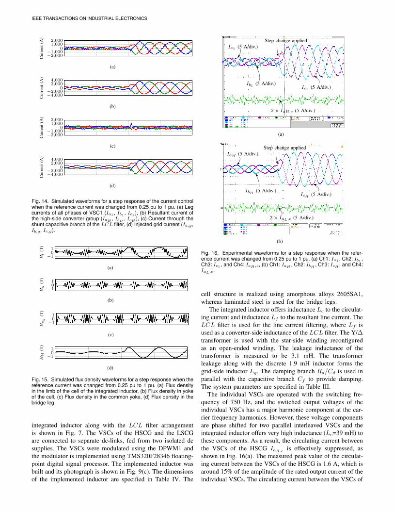
Fig. 14 shows the simulated current waveforms for a stepresponse of the current control when the reference current waschanged from 0.25 pu to 1 pu. The corresponding flux densitywaveforms for the phase a are also shown in Fig. 15. As itis evident for the Fig. 15(b), the dc component is avoided inthe circulating flux due to the simultaneous sampling of theparallel VSCs [25]. As a result, the inductor saturation duringthe transient is avoided. The waveform of the output currentof the HSCG has very small ripple component as shown inFig. 14(b), which proves the effectiveness of the integratedinductor.
The experimental results were obtained for the systemshown in Fig. 1. The electrical equivalent circuit of the
IEEE TRANSACTIONS ON INDUSTRIAL ELECTRONICS
−2,000−1,000
01,0002,000
Cur
rent
(A)
(a)
−4,000−2,000
02,0004,000
Cur
rent
(A)
(b)
−2,000−1,000
01,0002,000
Cur
rent
(A)
(c)
−4,000−2,000
02,0004,000
Cur
rent
(A)
(d)
Fig. 14. Simulated waveforms for a step response of the current controlwhen the reference current was changed from 0.25 pu to 1 pu. (a) Legcurrents of all phases of VSC1 (Ia1 , Ib1 , Ic1 ), (b) Resultant current ofthe high-side converter group (IaH , IbH , IcH ), (c) Current through theshunt capacitive branch of the LCL filter, (d) Injected grid current (Ia,g ,Ib,g , Ic,g).
−101
Bl
(T)
(a)
−101
By
(T)
(b)
−101
Bcy
(T)
(c)
−101
Bbl
(T)
(d)
Fig. 15. Simulated flux density waveforms for a step response when thereference current was changed from 0.25 pu to 1 pu. (a) Flux densityin the limb of the cell of the integrated inductor, (b) Flux density in yokeof the cell, (c) Flux density in the common yoke, (d) Flux density in thebridge leg.
integrated inductor along with the LCL filter arrangementis shown in Fig. 7. The VSCs of the HSCG and the LSCGare connected to separate dc-links, fed from two isolated dcsupplies. The VSCs were modulated using the DPWM1 andthe modulator is implemented using TMS320F28346 floating-point digital signal processor. The implemented inductor wasbuilt and its photograph is shown in Fig. 9(c). The dimensionsof the implemented inductor are specified in Table IV. The
Ia1 (5 A/div.)Step change applied
Ib1 (5 A/div.)Ic1 (5 A/div.)
2× IaH,c (5 A/div.)
(a)
IaH (5 A/div.)Step change applied
IbH (5 A/div.)IcH (5 A/div.)
2× IaL,c (5 A/div.)
(b)
Fig. 16. Experimental waveforms for a step response when the refer-ence current was changed from 0.25 pu to 1 pu. (a) Ch1: Ia1 , Ch2: Ib1 ,Ch3: Ic1 , and Ch4: IaH ,c, (b) Ch1: IaH , Ch2: IbH , Ch3: IcH , and Ch4:IaL,c.
cell structure is realized using amorphous alloys 2605SA1,whereas laminated steel is used for the bridge legs.
The integrated inductor offers inductance Lc to the circulat-ing current and inductance Lf to the resultant line current. TheLCL filter is used for the line current filtering, where Lf isused as a converter-side inductance of the LCL filter. The Y/∆transformer is used with the star-side winding reconfiguredas an open-ended winding. The leakage inductance of thetransformer is measured to be 3.1 mH. The transformerleakage along with the discrete 1.9 mH inductor forms thegrid-side inductor Lg . The damping branch Rd/Cd is used inparallel with the capacitive branch Cf to provide damping.The system parameters are specified in Table III.
The individual VSCs are operated with the switching fre-quency of 750 Hz, and the switched output voltages of theindividual VSCs has a major harmonic component at the car-rier frequency harmonics. However, these voltage componentsare phase shifted for two parallel interleaved VSCs and theintegrated inductor offers very high inductance (Lc=39 mH) tothese components. As a result, the circulating current betweenthe VSCs of the HSCG IaH,c
is effectively suppressed, asshown in Fig. 16(a). The measured peak value of the circulat-ing current between the VSCs of the HSCG is 1.6 A, which isaround 15% of the amplitude of the rated output current of theindividual VSCs. The circulating current between the VSCs of
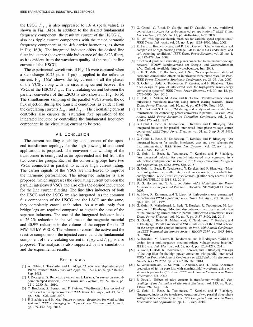
IEEE TRANSACTIONS ON INDUSTRIAL ELECTRONICS
the LSCG IaL,cis also suppressed to 1.6 A (peak value), as
shown in Fig. 16(b). In addition to the desired fundamentalfrequency component, the resultant current of the HSCG IaHalso has ripple current components with the major harmonicfrequency component at the 4th carrier harmonics, as shownin Fig. 16(b). The integrated inductor offers the desired linefilter inductance (converter-side inductance of the LCL filter),as it is evident from the waveform quality of the resultant linecurrent of the HSCG.
The experimental waveforms of Fig. 16 were captured whena step change (0.25 pu to 1 pu) is applied in the referencecurrent. Fig. 16(a) shows the leg current of all the phasesof the VCS1, along with the circulating current between theVSCs of the HSCG IaH ,c. The circulating current between theparallel converters of the LSCG is also shown in Fig. 16(b).The simultaneous sampling of the parallel VSCs avoids the dcflux injection during the transient conditions, as evident fromthe circulating currents IaH ,c and IaL,c. The circulating currentcontroller also ensures the saturation free operation of theintegrated inductor by controlling the fundamental frequencycomponent in the circulating current to be zero.
VII. CONCLUSION
The current handling capability enhancement of the open-end transformer topology for the high power grid-connectedapplications is proposed. The converter-side winding of thetransformer is configured as an open-ended and fed from thetwo converter groups. Each of the converter groups have twoVSCs connected in parallel to achieve high current rating.The carrier signals of the VSCs are interleaved to improvethe harmonic performance. The integrated inductor is alsoproposed, which suppresses the circulating current between theparallel interleaved VSCs and also offer the desired inductancefor the line current filtering. The line filter inductors of boththe HSCG and the LSCG are also integrated. As the commonflux components of the HSCG and the LSCG are the same,they completely cancel each other. As a result, only fourbridge legs are required compared to eight in the case of theseparate inductors. The use of the integrated inductor leadsto 26.2% reduction in the volume of the magnetic materialand 40.9% reduction in the volume of the copper for the 12MW, 3.3 kV WECS. The scheme to control the active and thereactive component of the injected current and the fundamentalcomponent of the circulating current in IaH,c and IaL,c is alsoproposed. The analysis is also supported by the simulationsand the experimental results.
REFERENCES
[1] A. Nabae, I. Takahashi, and H. Akagi, “A new neutral-point-clampedPWM inverter,” IEEE Trans. Ind. Appl., vol. IA-17, no. 5, pp. 518–523,Sep. 1981.
[2] J. Rodriguez, S. Bernet, P. Steimer, and I. Lizama, “A survey on neutral-point-clamped inverters,” IEEE Trans. Ind. Electron., vol. 57, no. 7, pp.2219–2230, Jul. 2010.
[3] T. Bruckner, S. Bernet, and P. Steimer, “Feedforward loss control ofthree-level active npc converters,” IEEE Trans. Ind. Appl., vol. 43, no. 6,pp. 1588–1596, Nov. 2007.
[4] F. Blaabjerg and K. Ma, “Future on power electronics for wind turbinesystems,” IEEE J. Emerging Sel. Topics Power Electron., vol. 1, no. 3,pp. 139–152, Sep. 2013.
[5] G. Grandi, C. Rossi, D. Ostojic, and D. Casadei, “A new multilevelconversion structure for grid-connected pv applications,” IEEE Trans.Ind. Electron., vol. 56, no. 11, pp. 4416–4426, Nov. 2009.
[6] E. Levi, “Multiphase electric machines for variable-speed applications,”IEEE Trans. Ind. Appl., vol. 55, no. 5, pp. 1893–1909, May. 2008.
[7] K. Fujii, P. Koellensperger, and R. De Doncker, “Characterization andcomparison of high blocking voltage IGBTs and IEGTs under hard- andsoft-switching conditions,” IEEE Trans. Power Electron., vol. 23, no. 1,pp. 172–179, Jan. 2008.
[8] “Technical guidline: Generating plants connected to the medium-voltagenetwork.” BDEW Bundesverband der Energie- und Wasserwirtschafte.V., [Online]. Available: http://www.bdew.de, Jun. 2008.
[9] S. K. T. Miller, T. Beechner, and J. Sun, “A comprehensive study ofharmonic cancellation effects in interleaved three-phase vscs,” in Proc.IEEE Power Electronics Specialists Conference, pp. 29–35, Jun. 2007.
[10] G. Gohil, L. Bede, R. Teodorescu, T. Kerekes, and F. Blaabjerg, “Linefilter design of parallel interleaved vscs for high-power wind energyconversion systems,” IEEE Trans. Power Electron., vol. 30, no. 12, pp.6775–6790, Dec. 2015.
[11] F. Ueda, K. Matsui, M. Asao, and K. Tsuboi, “Parallel-connections ofpulsewidth modulated inverters using current sharing reactors,” IEEETrans. Power Electron., vol. 10, no. 6, pp. 673–679, Nov. 1995.
[12] I. G. Park and S. I. Kim, “Modeling and analysis of multi-interphasetransformers for connecting power converters in parallel,” in Proc. 28thAnnual IEEE Power Electronics Specialists Conference, vol. 2, pp.1164–1170 vol.2, 1997.
[13] G. Gohil, L. Bede, R. Teodorescu, T. Kerekes, and F. Blaabjerg, “Anintegrated inductor for parallel interleaved three-phase voltage sourceconverters,” IEEE Trans. Power Electron., vol. 31, no. 5, pp. 3400–3414,May. 2016.
[14] G. Gohil, L. Bede, R. Teodorescu, T. Kerekes, and F. Blaabjerg, “Anintegrated inductor for parallel interleaved vscs and pwm schemes forflux minimization,” IEEE Trans. Ind. Electron., vol. 62, no. 12, pp.7534–7546, Dec. 2015.
[15] G. Gohil, L. Bede, R. Teodorescu, T. Kerekes, and F. Blaabjerg,“An integrated inductor for parallel interleaved vscs connected in awhiffletree configuration,” in Proc. IEEE Energy Conversion Congressand Exposition, pp. 5952–5959, Sep. 2015.
[16] G. Gohil, L. Bede, R. Teodorescu, T. Kerekes, and F. Blaabjerg, “Mag-netic integration for parallel interleaved vscs connected in a whiffletreeconfiguration,” IEEE Trans. Power Electron., [Online early access], DOI:10.1109/TPEL.2015.2514182, 2016.
[17] D. G. Holmes and T. A. Lipo, Pulse Width Modulation for PowerConverters: Principles and Practice. Hoboken, NJ: Wiley-IEEE Press,2003.
[18] A. Hava, R. Kerkman, and T. Lipo, “A high-performance generalizeddiscontinuous PWM algorithm,” IEEE Trans. Ind. Appl., vol. 34, no. 5,pp. 1059–1071, 1998.
[19] G. Gohil, R. Maheshwari, L. Bede, T. Kerekes, R. Teodorescu, M. Lis-erre, and F. Blaabjerg, “Modified discontinuous pwm for size reductionof the circulating current filter in parallel interleaved converters,” IEEETrans. Power Electron., vol. 30, no. 7, pp. 3457–3470, Jul. 2015.
[20] G. Gohil, L. Bede, R. Maheshwari, R. Teodorescu, T. Kerekes, andF. Blaabjerg, “Parallel interleaved VSCs: influence of the PWM schemeon the design of the coupled inductor,” in Proc. 40th Annual Conferenceon IEEE Industrial Electronics Society, IECON 2014, pp. 1693–1699,Oct. 2014.
[21] A. Rockhill, M. Liserre, R. Teodorescu, and P. Rodriguez, “Grid-filterdesign for a multimegawatt medium-voltage voltage-source inverter,”IEEE Trans. Ind. Electron., vol. 58, no. 4, pp. 1205–1217, 2011.
[22] G. Gohil, L. Bede, R. Teodorescu, T. Kerekes, and F. Blaabjerg, “Designof the trap filter for the high power converters with parallel interleavedVSCs,” in Proc. 40th Annual Conference on IEEE Industrial ElectronicsSociety, IECON 2014, pp. 2030–2036, Oct. 2014.
[23] K. Venkatachalam, C. Sullivan, T. Abdallah, and H. Tacca, “Accurateprediction of ferrite core loss with nonsinusoidal waveforms using onlysteinmetz parameters,” in Proc. IEEE Workshop on Computers in PowerElectronics, Jun. 2002.
[24] P. Dowell, “Effects of eddy currents in transformer windings,” Pro-ceedings of the Institution of Electrical Engineers, vol. 113, no. 8, pp.1387–1394, Aug. 1966.
[25] G. Gohil, L. Bede, R. Teodorescu, T. Kerekes, and F. Blaabjerg,“Integrated inductor for interleaved operation of two parallel three-phasevoltage source converters,” in Proc. 17th European Conference on PowerElectronics and Applications, pp. 1–10, Sep. 2015.